
A conventional transformer transfers power through a magnetic field and changes the relationship between voltage and current. In an AC distribution system it normally performs this task at the grid frequency. A solid-state transformer (SST) combines power-electronic conversion with a transformer operating at a higher internal frequency, allowing additional control of its electrical ports.
The useful question is not whether an SST is universally better than a conventional transformer. It is which application needs its particular combination of isolation, conversion and control, and whether those functions justify the additional equipment and losses.
This article introduces those choices. The three-stage SST system guide develops a complete learning route through circuit analysis, modelling, control, hardware design and integration.
1. Begin with the function of a transformer
For an ideal two-winding transformer, let the turns ratio be n = Np/Ns and define secondary current positive out of the secondary winding towards the load. Then the magnitudes satisfy
\[\frac{V_p}{V_s}=n,\qquad \frac{I_s}{I_p}=n,\qquad P_p=P_s. \tag{1}\]A real transformer additionally has winding resistance, leakage inductance, finite magnetising inductance and core loss. It does not independently regulate its input power factor, create a DC port or impose an arbitrary output waveform. Those functions require other equipment.
An SST introduces controlled switching stages. The internal transformer remains a physical magnetic component: its winding arrangement provides isolation and its flux must obey volt-second constraints. A higher operating frequency can reduce the magnetic size required for a given applied voltage and flux swing, but insulation, loss, cooling and electromagnetic interference still constrain the design.
2. One name covers several architectures
For clarity, this series uses the following functional classification.
| Architecture | Basic interpretation |
|---|---|
| Single stage | Integrated AC conversion and isolation without two independently buffered DC links |
| Two stages | Two principal conversion stages with one intermediate DC link; arrangements differ |
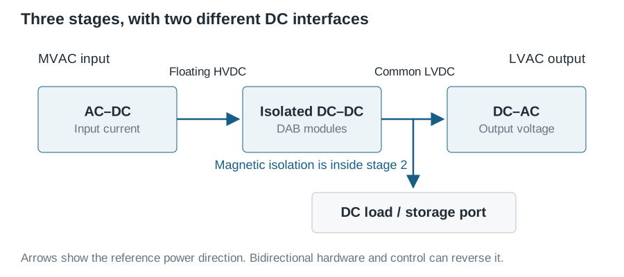
| Three stages | AC–DC front end, isolated DC–DC stage and DC–AC output, with DC links on both sides of the isolation stage |
The block diagram matters more than the label. A complete three-stage AC-to-AC path is
MVAC → AC–DC → high-side DC links → isolated DC–DC → LVDC → DC–AC → LVAC.
For a DC-only application, the required output can be taken from the LVDC bus. There is no need to add an AC output stage solely to match the three-stage diagram. Also, a modular front end can have separate floating high-side DC links rather than one externally accessible MVDC bus.
These distinctions are developed in the architecture chapter. They correct a common source of confusion: an MVAC-to-DC supply and a complete AC-to-AC SST need not contain the same stages.
3. Match the application to its ports
| Application | Useful interfaces and functions | Questions that determine the design |
|---|---|---|
| Distribution and local AC supply | MVAC input, regulated LVAC output, optional DC port | Voltage quality, overload capability, grounding, protection and service continuity |
| DC data-centre distribution | MVAC input and an isolated DC output | Conversion loss, load steps, redundancy, DC fault interruption and maintainability |
| High-power vehicle charging | MVAC input, isolated DC distribution and downstream charger interfaces | Wide load range, isolation arrangement, modular scaling and cooling |
| Storage and microgrids | AC and DC interfaces with controlled power flow | Energy availability, voltage/frequency responsibility and mode transitions |
| Traction and transport | Application-specific supply and vehicle-side ports | Mass, insulation, vibration, supply variation and thermal cycling |
This table describes engineering motivations, not a claim that every application has adopted SSTs or requires the same topology. Each project must compare the SST against the complete conventional alternative, including the converters needed around its line-frequency transformer.
4. An example: the path from an AC utility feed to a DC data hall
The original motivation for this article was the proposed use of higher-voltage DC distribution in AI data centres. NVIDIA’s published 800 VDC architecture discussion describes an approach to supplying future high-power computing infrastructure. It is an application proposal to examine, not a universal facility specification.
For an idealised 1 MW load, the current corresponding to 54 V is about 18.5 kA, while at 800 V it is 1.25 kA:
\[I=\frac{P}{V}. \tag{2}\]For equal resistance, conduction loss follows
\[P_{\mathrm{Cu}}=I^2R. \tag{3}\]This comparison illustrates the incentive to raise distribution voltage. It does not establish the total-system efficiency, because the conductor arrangement, conversion stages, insulation and protection also change.
An isolated MVAC-to-DC SST could feed the distribution bus. Downstream converters would still provide the rails required by servers and processors. A conventional line-frequency transformer followed by rectifiers is another possible route. The evaluation must include conversion efficiency over the actual load profile, fault handling, maintenance and redundancy.
The 800 V application is separate from the 48 V laboratory bus used in our teaching series. The lower-voltage example is selected to study the architecture and control; it is not an 800 V design scaled only by changing a source parameter.
5. Why modularity matters
A modular converter divides electrical stress and power among repeated cells. Series connections distribute voltage; parallel connections distribute current. The arrangement also determines where isolation is needed and which balancing variables must be controlled.
For an ideal group of equally loaded modules,
\[V_{\mathrm{series}}=\sum_{k=1}^{N}V_k,\qquad I_{\mathrm{parallel}}=\sum_{k=1}^{N}I_k. \tag{4}\]Equal loading does not happen automatically. Device tolerances, unequal capacitor energy, timing differences and thermal variation affect sharing. The modular integration chapter therefore treats balancing and startup as part of the design, rather than as wiring details.
As one practical research example, Awal et al. describe a modular medium-voltage AC to low-voltage DC converter for charging, using input-series/output-parallel converter modules. It illustrates how the requested port voltage and power lead to a modular architecture.
6. Evaluate the complete system
An SST may provide controlled input current, regulated output voltage, isolation and bidirectional power transfer when the selected converters and protection support those functions. Those capabilities have to be purchased with semiconductor devices, gate drives, sensors, control hardware and cooling.
Compare candidates using the same requirements:
- Loss across the mission profile, including auxiliaries and standby operation.
- Insulation and common-mode stress at every module and external port.
- Fault current paths, interruption capability and stored energy.
- Overload behaviour, thermal limits and recovery after disturbances.
- Reliability, replacement procedures and the effect of a failed module.
- Source and load interactions, including weak grids and constant-power loads.
Claims about smaller size or improved efficiency should state the comparison boundary and supporting measurements. A smaller high-frequency transformer alone does not demonstrate a smaller complete installation.
7. Follow the design through its three stages
The series uses a CHB front end, one DAB per floating cell and a central LVAC inverter. Begin with the shared specification and system guide, then study the AC–DC front end, DAB isolation stage and DC–AC output stage.
The final integration chapter combines them using explicit energy balances, control ownership and test milestones. The current articles are an analytical teaching draft. Prototype measurements and downloadable native design projects should be added as they are completed and verified.