
The output stage converts the common LVDC bus into a controlled AC port. Its control objective depends on what is connected to that port. A stand-alone load needs an established voltage and frequency. Connection to an existing AC system introduces synchronisation, power exchange and network dynamics.
We first develop an LC-filtered voltage source using the shared SST specification: a 48 V bus, 24 V line-to-line RMS output, 50 Hz and 600 W. The baseline is an isolated, three-wire laboratory circuit with a balanced 0.96 Ω star load. The numerical design is preliminary; no native simulation project, validated PCB or measured waveform is supplied in this draft.
1. Begin with the bridge and current paths
Each of three half bridges connects a phase pole either to the positive or negative DC rail. The upper and lower devices require complementary control and dead time. Their reverse-current paths let inductor current continue when the applied voltage changes. A series inductor limits current ripple; a shunt capacitor diverts switching-frequency current away from the load.
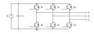
The balanced star load has its own floating star point; neither star point is connected to a DC rail. Per-phase equations below use the zero-sequence-free representation. A neutral-connected or four-wire system needs a separate zero-sequence model and a suitable return path.
If \(s_a,s_b,s_c\in\{0,1\}\) denote upper-switch states, the differential phase voltage is
\[u_a=V_b\left(s_a-\frac{s_a+s_b+s_c}{3}\right). \tag{1}\]This removes the common-mode voltage. For balanced sinusoidal PWM with phase references \(m_a+m_b+m_c=0\) and duties \(d_a=(1+m_a)/2\), averaging gives
\[\overline u_a=\frac{V_bm_a}{2},\qquad V_{LL,\mathrm{rms}}=\frac{\sqrt3}{2\sqrt2}mV_b. \tag{2}\]Here m is the sinusoidal modulation amplitude. Ignoring filter drops, 24 V from 48 V requires \(m=0.8165\). PWM commands the bridge voltage, so the actual modulation must also supply the inductor voltage and winding drop.
2. Size a first LC filter
Use preliminary per-phase values \(L_f=300\ \mu\mathrm H\), \(r_f=30\ \mathrm{m}\Omega\) and \(C_f=22\ \mu\mathrm F\). The capacitance is the value of each star-connected capacitor, not a delta-equivalent value. The unloaded ideal resonance is
\[f_{LC}=\frac{1}{2\pi\sqrt{L_fC_f}}=1.96\ \mathrm{kHz}. \tag{3}\]It lies above the 50 Hz fundamental and below the 20 kHz switching frequency. This frequency separation alone does not establish attenuation or stability: load damping, capacitor ESR, digital delay and control must also be included.
At the rated resistive load,
\[V_{\mathrm{ph,rms}}=\frac{24}{\sqrt3}=13.86\ \mathrm V,\qquad I_{o,\mathrm{rms}}=\frac{13.86}{0.96}=14.43\ \mathrm A, \qquad I_{o,\mathrm{pk}}=20.41\ \mathrm A. \tag{4}\]The capacitor fundamental current is about 0.096 A RMS. Inductor and semiconductor sizing must include switching ripple, overload and temperature; a 20.4 A saturation limit would already be inadequate. Begin with a current capability above the calculated peak and determine the required margin from the switched waveform and protection response. The assumed winding resistance dissipates approximately 6.25 W per phase at rated RMS current, making thermal design consequential even at this voltage.
3. Derive the physical model before transforming it
Let \(i_f\) flow from bridge to output and \(i_o\) from output to load. For either stationary αβ component, Kirchhoff’s laws give
\[L_f\dot i_f=u-r_fi_f-v_o,\qquad C_f\dot v_o=i_f-i_o. \tag{5}\]The first equation accounts for inductor voltage; the second accounts for capacitor current. Eliminating current gives
\[L_fC_f\ddot v_o+r_fC_f\dot v_o+v_o =u-L_f\dot i_o-r_fi_o. \tag{6}\]For an independently specified load-current disturbance,
\[\frac{\hat v_o}{\hat u}=\frac{1}{L_fC_fs^2+r_fC_fs+1},\qquad \frac{\hat v_o}{\hat i_o}=\frac{-(L_fs+r_f)}{L_fC_fs^2+r_fC_fs+1}. \tag{7}\]A resistor is not an independent current source: substituting \(i_o=v_o/R\) changes the voltage-plant denominator to \(L_fC_fs^2+(r_fC_f+L_f/R)s+1+r_f/R\). This distinction matters when comparing load-step simulations and frequency responses.
4. Transform sinusoidal states into steady quantities
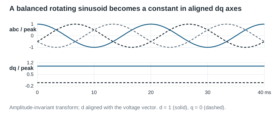
The dq companion derives the amplitude-invariant transform and its signs. Its d axis aligns with the desired output voltage and its q axis uses the negative-sine convention. Applying it to both filter equations yields
\[L_f\dot i_d=u_d-r_fi_d-v_d+\omega L_fi_q,\qquad L_f\dot i_q=u_q-r_fi_q-v_q-\omega L_fi_d, \tag{8}\] \[C_f\dot v_d=i_d-i_{o,d}+\omega C_fv_q,\qquad C_f\dot v_q=i_q-i_{o,q}-\omega C_fv_d. \tag{9}\]The cross terms come from rotating coordinates, not extra circuit components. Establish \(\dot\theta=2\pi50\) internally for this stand-alone test. The voltage references are \(v_d^*=\sqrt2(24/\sqrt3)=19.60\ \mathrm V\) and \(v_q^*=0\). At steady state the inverter also supplies \(i_q=\omega C_fv_d=0.135\ \mathrm A\) to the filter capacitor, even though the load has zero reactive current. Substituting these currents into the steady inductor equations gives a required bridge modulation of approximately 0.845, including the nominal filter drop. Bus-voltage sag and transients consume the remaining modulation margin.
5. Close the inductor-current loops
Define errors \(e_d=i_d^*-i_d\) and \(e_q=i_q^*-i_q\), and PI outputs \(w_d=K_{p,i}e_d+K_{i,i}\int e_d\,dt\), with the same form on q. Command
\[u_d^*=v_d-\omega L_fi_q+w_d,\qquad u_q^*=v_q+\omega L_fi_d+w_q. \tag{10}\]Substitution cancels capacitor-voltage disturbance and coordinate coupling, leaving \(L_f\dot i_d+r_fi_d=w_d\) on each axis. This ideal cancellation assumes accurate sensing, parameters and negligible delay. The remaining plant is \(1/(L_fs+r_f)\). Choose
\[K_{p,i}=L_f\omega_{c,i},\qquad K_{i,i}=r_f\omega_{c,i}. \tag{11}\]For a tentative 1 kHz crossover, these are 1.885 V/A and 188.5 V/(A·s). Nominal pole cancellation makes the continuous-time open loop \(\omega_{c,i}/s\). With a provisional 75 µs total delay, delay alone subtracts 27° at 1 kHz, leaving about 63° nominal phase margin in that simplified model. Verify the actual sampled loop with sensor dynamics, parameter uncertainty and PWM saturation before using these gains.
6. Close the output-voltage loops
Let \(z_d=K_{p,v}(v_d^*-v_d)+K_{i,v}\int(v_d^*-v_d)dt\), with the corresponding q expression. Load-current feedforward and capacitor decoupling give
\[i_d^*=i_{o,d}-\omega C_fv_q+z_d,\qquad i_q^*=i_{o,q}+\omega C_fv_d+z_q. \tag{12}\]With ideal fast current tracking, \(C_f\dot v_d=z_d\) and similarly on q. The characteristic polynomial is therefore
\[C_fs^2+K_{p,v}s+K_{i,v}=0, \qquad K_{p,v}=2\zeta\omega_nC_f,\qquad K_{i,v}=C_f\omega_n^2. \tag{13}\]For \(\zeta=0.707\) and \(f_n=100\ \mathrm{Hz}\), the gains are 0.0195 A/V and 8.69 A/(V·s). Natural frequency is not loop crossover. The full design retains the closed current-loop dynamics; without load-current measurement, omit that feedforward and redesign for the resulting load-dependent plant.
Limit the current-reference vector before passing it to the inner loop. Limit bridge voltage to the available modulation region, and prevent both integrators from accumulating error while their respective actuators are limited. Ramp the voltage reference at startup. Current limiting necessarily permits output-voltage deviation when the load asks for more than the inverter can supply.
7. Change the objective for grid-following operation
A grid-following controller measures an existing AC voltage and estimates its angle, commonly using a PLL. It then controls injected current. With the d axis aligned to that voltage and positive current from inverter to grid,
\[P=\frac32V_di_d,\qquad Q=-\frac32V_di_q, \qquad i_d^*=\frac{2P^*}{3V_d},\qquad i_q^*=-\frac{2Q^*}{3V_d}. \tag{14}\]A simple L-filter grid model follows the current equations above with \(v_o\) replaced by grid voltage. An LC filter plus grid-side inductance becomes an LCL network; its resonance and damping must be modelled explicitly. A grid-current loop cannot be assumed equivalent to the inductor-current loop already derived.
Grid-forming describes voltage-source behaviour and can also apply while connected to a grid. Coordinated power sharing, synchronisation and current limiting are then additional design problems. Imperix’s implementation note provides a practical example of cascaded voltage/current control and distinguishes the two control behaviours. The isolated stand-alone exercise here is an entry point, not a complete grid-interconnection design.
8. Build evidence from simulation to the bench
In PLECS, begin with a stiff 48 V source, an averaged three-phase bridge, the specified LC filter and balanced resistors. Verify open-loop amplitude and the analytical steady-state dq currents. Add the current loop before the voltage loop; then replace the averaged bridge with 20 kHz switching, dead time and sampled control. Apply a 300 W to 600 W load step, bus-voltage variation and load removal. Inspect inductor peak current, voltage recovery, modulation limits and both integrator states.
In Simulink, retain the same physical parameters and transform definitions, and represent ADC, computation and PWM timing explicitly. LTspice can investigate one leg’s switching transient, driver and sensing circuit. These are model-construction instructions; native projects remain to be developed.
For KiCad hardware, place DC decoupling beside the bridge commutation loops, route gate returns deliberately and keep current-sensing references clear of switching-node currents. First verify gate timing with a limited DC supply, then establish balanced operation at reduced voltage before increasing the load. Record RMS voltage, distortion, inductor ripple, winding temperature and load-step recovery against the same simulation cases.
Finally replace the stiff bus by the six DAB outputs and common capacitor. The inverter’s power demand now perturbs the SST bus; system integration explains how the other stages replenish that energy. This closes the connection between an independently working inverter and a working SST.