
Three working converters do not automatically make a working solid-state transformer. Integration requires an explicit answer to three questions: where is energy stored, which controller regulates each storage element, and what happens when a power path becomes unavailable?
This chapter joins the AC–DC front end, DAB modules and AC output stage using the shared teaching specification. It is an analytical design draft; the gains and sequences below require switched-model and hardware validation.
1. Distinguish stages from modules
The three stages are AC–DC, isolated DC–DC and DC–AC. Repeating a module increases voltage or current capability without necessarily increasing the number of functional stages.
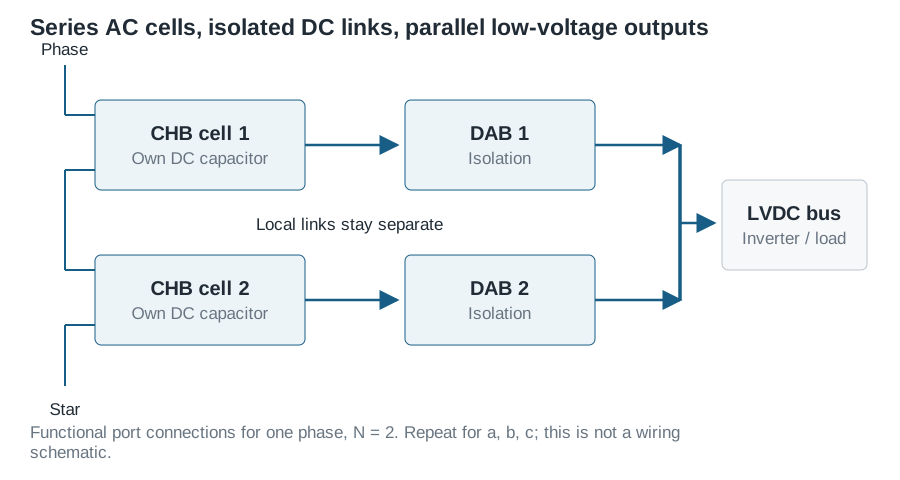
Our CHB has two series AC-connected cells per input phase and six floating 48 V DC links. Six 100 W DABs feed one 48 V bus. Their primary links remain electrically separate; their isolated secondary DC terminals are connected in parallel. A central inverter supplies 24 V line-to-line RMS, 50 Hz, to a balanced three-wire load.
For one phase, the averaged bridge voltage is
\[u_a=\sum_{k=1}^{2}m_{a,k}v_{h,a,k},\qquad |m_{a,k}|\leq1.\tag{1}\]Two 48 V cells provide an ideal 96 V peak synthesis limit. The 48 V line-to-line input has a 39.19 V phase peak, giving approximately 0.408 nominal utilisation before inductor drop. Series connection provides voltage capability; parallel isolated outputs share current. Awal et al. give an external example of modular input-series/output-parallel conversion.
2. Begin with energy conservation
Let positive power flow from the input source to the output load. Define cell energy and bus energy by
\[E_{j,k}=\frac12C_hv_{h,j,k}^{2},\qquad E_b=\frac12C_bv_b^2,\tag{2}\]where j identifies input phase and k identifies a cell. With losses represented explicitly,
\[\dot E_{j,k}=p_{\mathrm{AFE},j,k}-p_{\mathrm{DAB,in},j,k}-p_{\ell,j,k},\qquad \dot E_b=\sum_{j,k}p_{\mathrm{DAB,out},j,k}-p_{\mathrm{inv}}-p_{\ell,b}.\tag{3}\]The six 2200 µF high-side capacitors store 15.21 J at 48 V; the 4700 µF bus stores 5.41 J. Only the energy between permitted voltage limits is usable. If bus input disappears while a 600 W load remains constant, the ideal time to fall from 48 V to 44 V is
\[\Delta t=\frac{C_b(48^2-44^2)}{2P}=1.44\ \mathrm{ms}.\tag{4}\]Thus supervisory software alone cannot guarantee uninterrupted output after source loss. The required response time, available energy and hardware current limits must agree.
3. Give every controller one responsibility
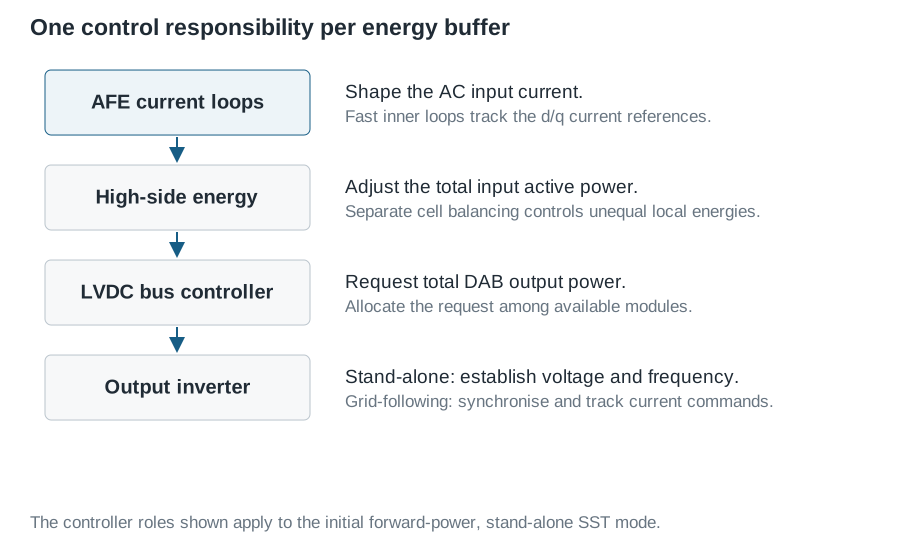
In the baseline stand-alone-output mode, the AFE total-energy loop regulates the sum of the six high-side energies by commanding source active current. AFE current loops track that command. Within each phase, bounded zero-sum AFE power corrections equalise its two cell energies. One bus-voltage supervisor commands the sum of DAB output currents. The inverter establishes AC voltage and frequency.
The front-end chapter derives within-phase correction: a low-energy cell receives more input power, while its neighbour receives less, leaving their total phase-voltage command unchanged.
Between-phase balancing needs another degree of freedom. Define filtered branch energies
\[E_j=\sum_kE_{j,k},\qquad \bar E=\frac13\sum_jE_j,\qquad \Delta P_j=k_E(E_j-\bar E).\tag{5}\]Use filtering that rejects the expected 100 Hz branch-energy ripple. Allocate DAB current according to
\[i_{j,k}^{*}=\frac{I_\Sigma^{*}}{6}+\frac{\Delta P_j}{2v_b},\qquad \sum_{j,k}i_{j,k}^{*}=I_\Sigma^{*}.\tag{6}\]A high-energy branch therefore exports more DAB power. Under ideal conversion and equal average AFE branch powers, its differential energy obeys approximately \(\dot{(E_j-\bar E)}=-k_E(E_j-\bar E)\). This establishes the correction sign. Loss mismatch, filtering and current-loop dynamics modify this approximation.
Enable this allocation only above a defined bus-voltage threshold. Saturation requires redistribution among modules with remaining capacity; independently clipping commands destroys the zero-sum property. Report any unmet total current demand to the bus supervisor and apply anti-windup. Near zero power, forward-only limits can remove balancing authority.
4. Derive the common-bus voltage loop
Assume DAB current tracking is sufficiently fast. If the inverter regulates its output voltage while supplying fixed resistors, its input behaves approximately as a constant-power load over the frequency range where that regulation is effective. Neglect losses for the following derivation:
\[C_b\frac{dv_b}{dt}=I_\Sigma-\frac{P}{v_b}.\tag{7}\]Linearise about \(V_b\) and P:
\[(C_bs-g)\hat v_b=\hat I_\Sigma-\frac{\hat P}{V_b},\qquad g=\frac{P}{V_b^2}.\tag{8}\]Since load current decreases when voltage increases, the incremental load resistance is negative: \(r_{\mathrm{inc}}=-V_b^2/P=-3.84\ \Omega\) at 600 W. With fixed source current, the linearised bus has an unstable pole \(g/C_b=55.41\ \mathrm{s}^{-1}\). This conclusion applies to the stated constant-power approximation; it does not describe every frequency or operating mode of the inverter.
Let bus error be \(e=V_b^*-v_b\) and command
\[I_\Sigma^*=I_{\mathrm{ff}}+K_pe+K_i\int e\,dt.\tag{9}\]Treat feedforward as fixed for this local stability calculation. The characteristic polynomial and coefficient-matched gains are
\[C_bs^2+(K_p-g)s+K_i=0,\qquad K_p=g+2\zeta\omega_nC_b,\quad K_i=C_b\omega_n^2.\tag{10}\]For \(\zeta=0.8\) and \(\omega_n=2\pi(20)\ \mathrm{rad/s}\), the preliminary gains are 1.205 A/V and 74.22 A/(V·s). The simplified model is stable because \(K_p>g\) and \(K_i>0\). Natural frequency is not identical to crossover. Include DAB tracking dynamics, sensing filters, computation delay and inverter input impedance before accepting loop margins. A measured power feedforward changes the disturbance response and, if voltage-dependent, the small-signal model.
At rated power, \(I_\Sigma=12.5\ \mathrm A\) and each DAB supplies 2.083 A. The AFE energy loop can remain slower than this bus loop, with capacitor energy buffering their temporary mismatch.
5. Define mode changes explicitly
For a grid-connected output, one option retains the DAB bus supervisor and makes the inverter follow bounded P/Q commands. Another option assigns LVDC regulation to the grid inverter and operates DABs from power commands. In the second option, disable the DAB bus-voltage integrator and define the high-side energy/source-power coordination again. Integrator state transfer and reference ramps prevent command steps during either transition.
“Bidirectional” describes converter capability. It does not establish that a laboratory source can absorb regenerated power. Source limits, bus overvoltage thresholds and a verified energy-removal path must define what happens when power reverses or a load disconnects.
6. Commission through observable states
| State | Action and exit evidence |
|---|---|
| Off and checked | Confirm discharged links, sensor polarity, interlocks and independent floating supplies. |
| High-side precharge | Charge each floating capacitor through a designed current-limited path; verify every cell voltage before bypassing its precharge element. |
| AFE enabled | Establish input-current control and regulated mean cell energy with conservative limits. |
| LVDC precharge | Charge the common bus using a separately verified current-limited path or a dedicated DAB startup sequence. |
| DAB regulation | Transfer to current-command operation once bus voltage and voltage ratio enter the validated operating region. |
| AC output ramp | Establish output frequency and ramp voltage before applying rated load. |
| Run or fault | Enforce current, voltage, temperature and communication limits; execute the defined isolation/discharge sequence. |
Passive CHB charging alone does not guarantee equal 48 V cells. Likewise, normal steady-state SPS equations do not guarantee safe charging of an initially empty bus: voltage mismatch can produce transfer-inductor current even at zero phase shift. Model diode paths, initial flux, pulse timing and current limiting throughout startup. Blocking gate signals does not necessarily interrupt diode conduction.
7. Validate the assembled system
First join averaged stage models in Simulink and perturb one cell energy, input voltage and output load separately. Then use switched PLECS models to check current peaks, saturation, precharge and transitions. LTspice can resolve selected driver and commutation details.
For hardware, progress from one DAB to one phase branch and then the six-module system. Record every cell voltage, bus voltage, current-sharing error, source/output power and protective-state transition. Test a load reduction, a lost module and a delayed command at reduced power before increasing ratings. A failed series cell requires a designed bypass or shutdown policy; a failed parallel output requires fault isolation before continued operation can be assumed.
No native system model, verified PCB or experimental performance is claimed here. These equations, control assignments and test cases define the next engineering implementation of the complete SST.