
A solid-state transformer (SST) combines controlled power conversion with magnetic isolation. Understanding it requires two views: the switching circuits inside each module, and the energy exchanged between modules and ports. This series develops both views using one consistent example.
The aim is to progress from circuit equations to a scaled laboratory system. This page is the main guide. Begin with applications if the motivation is unfamiliar, then follow the three power-stage tutorials and the integration chapter.
Engineering draft. The specification below defines a teaching design, not a tested SST. Equations and numerical examples are analytical. Native PLECS/Simulink projects, a selected component BOM, production firmware and validated PCBs remain to be developed. Laboratory and medium-voltage requirements are distinguished throughout.
1. What the three stages mean
For this series, a three-stage AC-to-AC SST contains an AC–DC stage, an isolated DC–DC stage and a DC–AC stage. Stage count describes the conversion architecture; it does not count every transistor bridge or every repeated module.
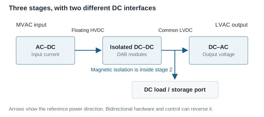
A single-stage architecture performs the required AC conversion and isolation without two independently buffered DC links. Two-stage arrangements retain one intermediate DC link; the location and combination of functions can differ. The three-stage arrangement provides separate input, isolation and output control interfaces, at the cost of more conversion hardware and energy-storage elements. Classification should always be accompanied by the actual block diagram.
An SST supplying only a DC load may end at the LVDC port. The LVAC inverter is then unnecessary for that service. Thus the data-centre application and the complete AC-to-AC teaching system are related configurations, not identical conversion chains.
2. The reference architecture
We select a star-connected, three-phase cascaded H-bridge (CHB) front end. Each phase contains N series-connected H-bridge AC terminals. Each bridge has its own floating DC capacitor and supplies one DAB. The isolated DAB outputs join a common LVDC bus. A central three-phase inverter supplies the LVAC port.
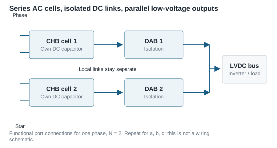
The vertical connections are functional port connections, not shared primary-side grounds. There are six separate high-side DC links when N = 2. They must not be wired together. “High side” identifies the primary side of the isolation barrier; in the scaled prototype its nominal voltage is only 48 V.
Input-series/output-parallel structures let modules share voltage on one side and current on the other. An example of this principle implemented with active-front-end and isolated converter modules is described by Awal et al.. Our numerical example is independently chosen and is not a reproduction of that prototype.
3. One specification for the entire series
| Quantity | Teaching-system value |
|---|---|
| Input source | Isolated three-phase laboratory source, 48 V line-to-line RMS, 50 Hz |
| CHB arrangement | N = 2 cells per phase; M = 3N = 6 cells total |
| Nominal cell DC voltage | 48 V per floating high-side link |
| Cell DC capacitance | 2200 µF effective per cell, preliminary |
| Nominal power per DAB | 100 W forward; reverse operation studied separately |
| Total nominal power | 600 W ideal transfer basis; losses require input headroom |
| DAB ratio | n = Np/Ns = 1 |
| DAB switching frequency | 50 kHz |
| DAB transfer inductance | 20 µH referred to the primary, total leakage plus external inductance |
| Common LVDC bus | 48 V, 4700 µF effective, preliminary |
| AFE and output switching | 20 kHz per bridge |
| LVAC output | 24 V line-to-line RMS, 50 Hz, three-wire balanced baseline |
| Output test load | Balanced star resistors, 0.96 Ω per phase at 600 W total |
The six 100 W allocations are lossless power bookkeeping. Delivering 600 W to the actual AC load requires each upstream stage to carry its share of downstream losses as well; final module ratings must include this headroom. For example, the preliminary output-inductor resistances alone dissipate about 18.75 W at nominal load.
These values preserve modularity while separating the learning exercise from direct public-grid or medium-voltage work. Start individual modules below rated power. A physical build still requires verified isolation, current limiting, discharge paths and device ratings.
With balanced unity-power-factor operation,
\[I_{g,\mathrm{rms}}=\frac{P}{\sqrt3 V_{g,LL}}=7.22\ \mathrm A, \qquad I_{o,\mathrm{rms}}=\frac{P}{\sqrt3 V_{o,LL}}=14.43\ \mathrm A. \tag{1}\]These are ideal rated currents; losses raise the required input power. They already show why the lower-voltage output needs substantial current capability.
The input phase-voltage peak is 39.19 V. Two 48 V full bridges can synthesise up to 96 V phase-branch voltage in the ideal averaged model. The nominal sinusoidal utilisation is therefore about 0.408 before the input-inductor voltage allowance. For the output two-level inverter under sinusoidal PWM,
\[V_{o,LL,\mathrm{rms}}=\frac{\sqrt3}{2\sqrt2}mV_b, \qquad m\approx0.816. \tag{2}\]Here \(V_b\) is the common bus and m is the peak sinusoidal modulation index. Filter drops and regulation headroom must be checked before accepting the operating envelope.
4. Follow power and stored energy
Positive power flows from the input AC source towards the LVAC load. Define the cell and bus energies as
\[E_k=\frac12 C_hv_{h,k}^2,\qquad E_b=\frac12 C_bv_b^2. \tag{3}\]Their averaged balances are
\[\dot E_k=p_{\mathrm{AFE},k}-p_{\mathrm{DAB,in},k}-p_{\mathrm{loss},h,k}, \tag{4}\] \[\dot E_b=\sum_{k=1}^{M}p_{\mathrm{DAB,out},k}-p_{\mathrm{inv}}-p_{\mathrm{DCload}}-p_{\mathrm{loss},b}. \tag{5}\]The capacitor stores a temporary power mismatch. It cannot continuously supply missing power. This observation determines the control hierarchy and the required response to an unavailable source.
5. Assign a clear control responsibility
For the initial forward-power, stand-alone-output operating mode, use the following division.
| Controller | Main responsibility |
|---|---|
| AFE fast current loops | Track input-current commands with the required phase relationship |
| AFE total-energy loop | Maintain the mean stored energy of the high-side links |
| Cell balancing loops | Correct differences between cell energies |
| One LVDC supervisor | Convert bus-voltage error into total DAB output-current demand |
| DAB module controllers | Follow assigned current/power commands within current and phase limits |
| Output inverter | Establish LVAC voltage and frequency, subject to current limits |
There is one supervising voltage controller for the shared LVDC bus in this arrangement. Multiple uncoordinated stiff voltage controllers are not the intended sharing method. System integration derives the energy and sharing loops and discusses an alternative assignment for grid-connected operation.
6. Read each power-stage tutorial
The AC–DC front-end article develops the bridge model, the input-current plant, high-side capacitor energy, control signs and voltage balancing.
The DAB article develops switching waveforms, phase-shift power transfer, current stress, the slow output model and control. Detailed algebra is in the DAB derivation; magnetic design has its own chapter.
The DC–AC article begins with an LC-filtered voltage source and extends to grid current control. The coordinate-transform tutorial defines every sign and scaling convention used by the AC stages.
7. From equations to an assembled system
Use PLECS for switched and averaged stage models, and Simulink for system control, sampled implementation and supervisory states. Use LTspice for selected driver, switching and analogue-sensing circuits. Each environment should consume the same parameter table; changing an inductance or ratio in one model must be recorded in the others.
Begin with one independently supplied DAB, then test one AFE cell and one output inverter. Assemble one input phase branch before completing the three-phase system. Validate the average energy flows before increasing power or enabling advanced modes.
For every milestone, preserve the model version, component assumptions, expected waveforms, observed waveforms and acceptance criteria. The integration chapter provides the startup sequence and a staged test plan. A correct steady-state simulation is one milestone; it does not establish the isolation, thermal performance or fault behaviour of hardware.
Further study
Robert W. Erickson and Dragan Maksimović, Fundamentals of Power Electronics, third edition, Springer, 2020, provides background on steady-state analysis, averaged modelling, control and magnetics. This series develops its own teaching example with explicit assumptions, intermediate derivation steps and checks against physical behaviour.