
The input stage controls the exchange of power between the AC source and the floating DC links. Its job is not simply to rectify voltage. It must shape input current, supply the downstream stages and keep the stored capacitor energies within their allowed ranges.
This chapter uses the series specification: two CHB cells per phase, 48 V per cell and 600 W total ideal power. First understand one bridge; then connect its AC port in series with the other bridges.
1. A bridge is a controllable AC voltage
A full bridge connects its AC terminals to a DC capacitor with either polarity. If its two ideal leg states are \(s_A,s_B\in\{0,1\}\), the bridge AC voltage is
\[u_k=(s_A-s_B)v_{h,k}. \tag{1}\]The possible levels are \(+v_{h,k},0,-v_{h,k}\). Complementary devices in a leg must never conduct simultaneously. Hardware dead time prevents overlap but introduces a current-dependent voltage error.
After switching-period averaging, define \(m_k=\langle s_A-s_B\rangle\). Then
\[u_k=m_kv_{h,k},\qquad -1\leq m_k\leq1. \tag{2}\]This equation defines m; it is not the duty of a single transistor. With N cells in one phase branch,
\[u_a=\sum_{k=1}^{N}m_{a,k}v_{h,a,k}. \tag{3}\]Use independent gate supplies, sensing and communication arrangements appropriate to the floating cell potentials. Series AC terminals do not imply series DC capacitors or a common primary ground.

2. Derive the input-current equation
Let input current be positive from source to converter. With phase inductance \(L_g\) and resistance \(r_g\),
\[L_g\frac{di_a}{dt}=v_{g,a}-r_gi_a-u_a. \tag{4}\]This phase equation assumes a consistent source/converter neutral reference. In the three-wire system a common-mode term may be needed in phase variables; it disappears from the zero-sequence-free dq equations below.
Increasing converter voltage u reduces the rate at which positive input current rises. This sign is essential when implementing the current controller.
Instantaneous bridge power received from the AC side is \(u_ki_a\). Neglecting bridge losses, its local capacitor obeys
\[C_hv_{h,k}\frac{dv_{h,k}}{dt}=u_ki_a-p_{\mathrm{DAB},k}. \tag{5}\]This equation explains why a cell with excessive outgoing DAB power loses voltage even if the total input power is correct.
3. Establish the steady operating point
For balanced source voltages and sinusoidal currents, define peak dq quantities using the stated transform. Align the d axis with the source voltage, so \(v_{g,q}=0\). Power into the converter is
\[P_g=\frac32V_{g,d}I_d,\qquad Q_g=-\frac32V_{g,d}I_q. \tag{6}\]Positive Q denotes absorbed inductive reactive power under this convention. Setting \(I_q=0\) gives unity displacement factor in the ideal balanced case; distortion must be assessed separately.
At 48 V line-to-line RMS, \(V_{g,d}=39.19\ \mathrm V\). The ideal 600 W operating point needs \(I_d=10.21\ \mathrm A\) peak, corresponding to 7.22 A RMS per phase. Include losses when computing the actual current reference.
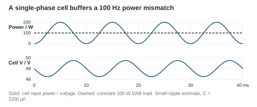
The average input power to each of six balanced cells is 100 W. Even when the total three-phase power is constant, each single-phase branch contains twice-line-frequency power pulsation. If a cell supplies approximately constant DAB power,
\[p_k(t)\approx P_k[1-\cos(2\omega_gt)], \qquad \Delta v_{h,\mathrm{pp}}\approx\frac{P_k}{\omega_gC_hV_h}. \tag{7}\]For 100 W, 50 Hz, 2200 µF and 48 V, this estimate is 3.01 V peak-to-peak. The derivation integrates the oscillating power into capacitor energy and uses small voltage ripple. It must be revised if the DAB deliberately transfers the 100 Hz pulsation to the common bus.
4. Obtain the dq current plant
Applying the chosen transform gives
\[L_g\dot i_d=v_{g,d}-r_gi_d-u_d+\omega_gL_gi_q, \tag{8}\] \[L_g\dot i_q=v_{g,q}-r_gi_q-u_q-\omega_gL_gi_d. \tag{9}\]Define PI outputs \(w_d=G_i(s)(i_d^*-i_d)\) and \(w_q=G_i(s)(i_q^*-i_q)\). Use voltage feedforward and decoupling:
\[u_d^*=v_{g,d}+\omega_gL_gi_q-w_d, \qquad u_q^*=v_{g,q}-\omega_gL_gi_d-w_q. \tag{10}\]With ideal decoupling and no saturation, each axis becomes
\[L_g\dot i+r_gi=w,\qquad G_{iw}(s)=\frac1{L_gs+r_g}. \tag{11}\]For \(G_i=K_p+K_i/s\), the characteristic polynomial is
\[L_gs^2+(r_g+K_p)s+K_i. \tag{12}\]One design method places the PI zero at the plant pole:
\[K_p=L_g\omega_c,\qquad K_i=r_g\omega_c. \tag{13}\]As a preliminary continuous-time example, choose \(L_g=1\ \mathrm{mH}\), \(r_g=0.1\ \Omega\) and \(f_c=500\ \mathrm{Hz}\). The gains are 3.142 V/A and 314.2 V/(A·s). These are voltage-command gains, before division by available bridge voltages.
This cancellation-based design assumes known resistance and ideal timing. Include ADC filters, PWM delay, parameter error and limits before accepting it. At 500 Hz, a 75 µs effective delay alone contributes about 13.5° phase lag. Verify the complete loop and sampled implementation.
5. Regulate total high-side energy
Define total capacitor energy
\[E_h=\sum_{k=1}^{M}\frac12C_hv_{h,k}^2. \tag{14}\]For the slow energy loop, neglect input-inductor energy dynamics and losses, and treat downstream power as a disturbance. Using the balanced fundamental power gives
\[\dot E_h=\frac32V_{g,d}i_d-P_{\mathrm{DAB,tot}}. \tag{15}\]With a much faster current loop, its local plant is approximately
\[\frac{\hat E_h(s)}{\hat i_d^*(s)}\approx\frac{3V_{g,d}}{2s}. \tag{16}\]The outer energy PI increases input d-current when stored energy is too low. If its output is current in amperes and its error is energy in joules, coefficient matching for damping ζ and natural frequency \(\omega_n\) yields
\[K_{p,E}=\frac{2\zeta\omega_n}{a},\qquad K_{i,E}=\frac{\omega_n^2}{a},\qquad a=\frac32V_{g,d}. \tag{17}\]For ζ = 0.707 and \(f_n=5\ \mathrm{Hz}\), the illustrative gains are approximately 0.756 A/J and 16.79 A/(J·s). These are not interchangeable with gains for a voltage-error controller. Filtering and the actual inner-loop response must be included in the final model.
Keep deliberate regulation of the mean energy separate from the natural 100 Hz cell ripple. A fast controller attempting to eliminate that ripple through the source-current command can degrade the input waveform.
6. Balance the cells
The total-energy controller cannot determine six independent capacitor energies. Additional balancing is required.
Within a phase branch, suppose the desired cell-power corrections satisfy \(\sum_k\Delta P_k=0\). One cycle-average voltage-allocation law is
\[\Delta u_k(t)=\frac{\Delta P_k}{I_{a,\mathrm{rms}}^2}i_a(t). \tag{18}\]It gives \(\langle\Delta u_ki_a\rangle=\Delta P_k\) and leaves the total phase-voltage command unchanged. A low-energy cell should receive a positive input-power correction. Limit the corrections, use a protected denominator and disable or change the strategy near zero current. There is no balancing authority through this expression when branch current is zero.
Balancing between phase branches requires further control freedom. For this teaching system, differential DAB power allocation can equalise phase energies: temporarily draw more power from a high-energy branch and less from a low-energy branch, while preserving total bus demand. Common-mode CHB voltage control is another approach. Implement one explicit coordination policy rather than letting several balancing loops counteract one another. Imperix TN165 provides an experimental CHB implementation distinguishing within-branch and between-branch balancing.
7. Modulation, simulation and implementation
Recover phase commands from the inverse dq transform. Allocate each phase command across its cells, add bounded balancing corrections and calculate \(m_k=u_k^*/v_{h,k}\). If a cell voltage falls, its available voltage decreases; normalisation and saturation must use the measured value.
First simulate one phase with two bridges, two separate DC capacitors and controlled DC loads representing the DAB inputs. Then add three-phase current control, total-energy control and the balancing policy. Start with synchronous carriers to inspect the waveform; introduce phase-shifted carriers as a documented modulation variant and measure the resulting ripple. The carrier relationship depends on the bipolar/unipolar modulation convention and must be defined with a timing diagram.
Inspect source current, summed bridge voltage, individual capacitor voltages, modulation limits and actual input power. Test unequal cell loads, a source-voltage change and a small intentional initial energy imbalance. A controller that only works with perfectly equal initial voltages has not demonstrated balancing.
For hardware, determine the inductor ripple from the actual PWM voltage sequence, then check saturation and copper loss. The 1 mH value above is a control-model starting point, not a completed magnetic design. Select capacitor ripple-current ratings, bridge devices, isolated gate supplies, precharge paths, sensors and fault interfaces before layout.
Bring up one bridge from a current-limited isolated source before making a series branch. Validate current polarity and gate timing at low power. Never use an earth-referenced probe connection to join floating cell grounds. Commission reverse power only with a source able to absorb it.
8. Acceptance evidence
Record RMS and peak input current, current spectrum, real/reactive power, cell-voltage ripple, transient maxima and balancing settling time. Specify the source impedance, operating power, controller rate and limits for every test. The values derived here are expected model quantities; no hardware results are claimed.
Continue to the DAB isolation stage or return to the system guide.