
The high-frequency transformer supplies galvanic isolation and voltage scaling inside the DAB stage. Its design begins with winding voltage and current waveforms. Power rating alone does not determine turns, core size or winding arrangement.
Use the series example: 48 V primary and secondary DC ports, 100 W per module, 50 kHz switching and \(n=N_p/N_s=1\). All inductances below are referred to the primary unless stated otherwise. The numerical exercise establishes preliminary constraints; it does not select a core, winding assembly or insulation system.
1. Integrate winding voltage to obtain flux
Let \(v_p(t)\) be voltage across the ideal transformer primary, excluding the voltage across separately represented leakage and external series inductance. Faraday’s law gives
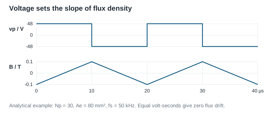
\[v_p=N_p\frac{d\Phi}{dt}=N_pA_e\frac{dB}{dt},\qquad \Delta B=\frac{1}{N_pA_e}\int v_p(t)\,dt.\tag{1}\]For a symmetric square winding voltage \(\pm V_p\) at switching frequency \(f_s\), one positive half-cycle moves flux from \(-B_{\mathrm{pk}}\) to \(+B_{\mathrm{pk}}\). Therefore
\[2B_{\mathrm{pk}}=\frac{V_p}{2f_sN_pA_e},\qquad N_p\geq\frac{V_p}{4f_sA_eB_{\mathrm{pk,allow}}}.\tag{2}\]The factor four follows from both the half-period and the peak-to-peak flux excursion. This expression assumes symmetric steady operation with zero flux offset. Check the actual winding voltage when the DAB voltage ratio, modulation or inductance placement changes.
As a numerical exercise, take \(A_e=80\ \mathrm{mm^2}=80\times10^{-6}\ \mathrm{m^2}\) and \(B_{\mathrm{pk,allow}}=0.10\ \mathrm T\):
\[N_p\geq\frac{48}{4(50\times10^3)(80\times10^{-6})(0.10)}=30,\qquad N_s=30.\tag{3}\]Thirty turns is the minimum under these nominal assumptions, with no allowance for voltage tolerance or reduced switching frequency. A 52.8 V winding voltage would require 33 turns at the same flux limit. The chosen 0.10 T is a design target, not a verified material limit; select it using temperature-dependent saturation and loss data.
2. Keep two inductances distinct
The DAB transfer inductance \(L_\sigma=20\ \mu\mathrm H\) carries the differential voltage between the bridges. Magnetising inductance \(L_m\) describes the current needed to establish core flux:
\[L_\sigma\frac{di_\sigma}{dt}=v_1-v_2',\qquad L_m\frac{di_m}{dt}=v_p.\tag{4}\]They are different elements of the equivalent circuit. The transfer inductance may combine measured leakage with an external inductor; do not count the same measured leakage twice. The external inductor needs its own saturation, energy and thermal design.
For the symmetric square voltage, magnetising current is triangular. If a trial design yields \(L_m=1\ \mathrm{mH}\),
\[\Delta i_{m,\mathrm{pp}}=\frac{V_p}{2f_sL_m}=0.48\ \mathrm A,\qquad I_{m,\mathrm{rms}}=\frac{\Delta i_{m,\mathrm{pp}}}{2\sqrt3}=0.139\ \mathrm A.\tag{5}\]The DAB’s nominal transfer current is approximately 2.23 A RMS in the ideal matched-voltage case. Add magnetising current waveform by waveform on the appropriate winding; its RMS does not generally add by ordinary arithmetic or root-sum-square because the currents are correlated. Verify magnetising inductance from the actual core, turns, gap and assembly.
3. Account for flux offset
Steady periodic flux requires zero net winding volt-seconds:
\[\int_0^{T_s}v_p(t)\,dt=0.\tag{6}\]Unequal pulse durations, device drops, startup or a control update can violate this condition. For net error \(\Delta\mathcal V\) in volt-seconds per cycle, flux offset changes by
\[\Delta B_{\mathrm{offset}}=\frac{\Delta\mathcal V}{N_pA_e}.\tag{7}\]Persistent error can drive the core towards saturation even when the symmetric flux excursion satisfies equation (2). Check pulse symmetry, startup timing and current-offset detection. A DC-blocking capacitor is one possible circuit measure, but changes resonances and transient behaviour and needs its own analysis.
4. Convert current waveforms into winding requirements
Choose conductor area using RMS current, allowable temperature rise and the available window. At 50 kHz, skin and proximity effects make winding arrangement relevant. A useful copper skin-depth estimate is
\[\delta=\sqrt{\frac{\rho}{\pi f\mu_0}}\approx0.30\ \mathrm{mm},\tag{8}\]using \(\rho=1.72\times10^{-8}\ \Omega\mathrm m\) at room temperature and \(f=50\ \mathrm{kHz}\). This estimate alone cannot choose strand diameter or predict AC resistance; the current waveform contains harmonics and the magnetic field depends on layer placement.
A harmonic winding-loss calculation is
\[P_{\mathrm{cu}}=I_{\mathrm{dc}}^2R_{\mathrm{dc}}+\sum_{h\geq1}I_{h,\mathrm{rms}}^2R_{\mathrm{ac}}(hf_s,T).\tag{9}\]Interleaving can reduce leakage and proximity loss while increasing interwinding capacitance. That tradeoff matters to a DAB that deliberately requires transfer inductance and to an SST exposed to common-mode switching. TI’s DAB design guide provides a practical reference for winding and magnetic-loss considerations.
5. Close the core-loss and thermal calculation
Obtain core loss from manufacturer data or a validated model for the selected material, flux waveform, frequency and temperature. A fitted sinusoidal loss expression must not be applied to arbitrary switching waveforms without justification.
As a first thermal estimate,
\[P_{\mathrm{mag}}=P_{\mathrm{core}}+P_{\mathrm{cu}}+P_{\mathrm{other}},\qquad \Delta T\approx R_\theta P_{\mathrm{mag}}.\tag{10}\]Thermal resistance depends on mounting, airflow and winding construction. Iterate turns, conductor placement and core choice until flux, window occupancy, loss and hot-spot temperature all meet the specified envelope. A volt-second calculation alone cannot establish a 100 W rating.
6. Design and verify the isolation boundary
In a medium-voltage CHB, a module can experience primary-to-secondary common-mode stress much greater than its local DC-link voltage. Derive insulation requirements from module position, grounding, transients and applicable equipment requirements. Clearance, creepage, dielectric tests, partial-discharge evaluation where applicable, and interwinding capacitance require a defined insulation specification; this low-voltage example supplies no medium-voltage spacing prescription.
Before full-power testing, verify turns ratio, polarity, magnetising inductance, short-circuit leakage under a documented test connection, and winding resistance. Check voltage integration for flux drift at reduced voltage, then compare winding current and temperature with calculations across the voltage-ratio range. Use isolation test methods appropriate to the intended equipment class.
The design record should contain the winding drawing, equivalent circuit, core/material data, loss estimate, insulation specification and measured results. These are the inputs needed before the transformer can become a verified component in the modular SST.