
The DAB power equation is useful only when its variables and assumptions are understood. This companion to the DAB tutorial derives it from the switching intervals, then constructs a model for control. The SST series guide explains where this stage belongs.
1. Define the circuit and the approximation
Both bridges generate symmetrical square waves with 50% duty. Initially, the DC voltages are constant within a switching cycle. Neglect losses, dead time, magnetising current and switching transitions. Define
\[n=\frac{N_p}{N_s},\qquad V_2'=nV_2,\qquad \omega_s=2\pi f_s,\qquad \theta=\omega_st. \tag{1}\]The total transfer inductance \(L_\sigma\) is referred to the primary. The current \(i_\sigma\) is positive from the primary bridge towards the transformer; positive power enters the secondary DC port. The secondary bridge waveform lags the primary by \(\phi\) radians. Begin with \(0\leq\phi\leq\pi\).
During the first half cycle, the primary bridge voltage is \(+V_1\). The referred secondary voltage is \(-V_2'\) before \(\phi\) and \(+V_2'\) afterwards. Therefore
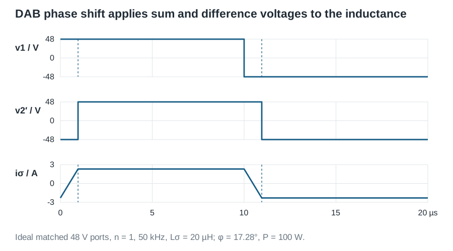
\[\frac{di_\sigma}{d\theta}= \begin{cases} \dfrac{V_1+V_2'}{\omega_sL_\sigma},&0<\theta<\phi,\\[6pt] \dfrac{V_1-V_2'}{\omega_sL_\sigma},&\phi<\theta<\pi. \end{cases} \tag{2}\]The first interval imposes the sum of the DC voltages across the inductance. The second imposes their difference. At matched voltages, the second slope is zero; at mismatched voltages it is not.
2. Determine the current endpoints
Write \(I_0=i_\sigma(0)\), \(I_\phi=i_\sigma(\phi)\) and \(I_\pi=i_\sigma(\pi)\). Integrating each slope gives
\[I_\phi=I_0+\frac{(V_1+V_2')\phi}{\omega_sL_\sigma},\qquad I_\pi=I_\phi+\frac{(V_1-V_2')(\pi-\phi)}{\omega_sL_\sigma}. \tag{3}\]Choose the symmetrical, zero-DC-current solution, for which \(I_\pi=-I_0\). This is an additional operating condition: an ideal lossless inductor can retain an arbitrary current offset, so periodicity alone does not eliminate DC bias. Combining the two intervals yields
\[-2I_0=\frac{(V_1-V_2')\pi+2V_2'\phi}{\omega_sL_\sigma}. \tag{4}\]Consequently,
\[\boxed{I_0=-\frac{(V_1-V_2')\pi+2V_2'\phi}{2\omega_sL_\sigma}},\qquad \boxed{I_\phi=\frac{-(V_1-V_2')\pi+2V_1\phi}{2\omega_sL_\sigma}},\qquad I_\pi=-I_0. \tag{5}\]Between these endpoints the current is linear. The second half cycle satisfies \(i_\sigma(\theta+\pi)=-i_\sigma(\theta)\). These relations completely specify the assumed steady waveform.
3. Integrate instantaneous power
The voltage and current both change sign after half a period, so their product repeats. The average secondary power is
\[P=\frac{1}{\pi}\left[-V_2'\int_0^\phi i_\sigma\,d\theta +V_2'\int_\phi^\pi i_\sigma\,d\theta\right]. \tag{6}\]Each current integral is the area of a trapezoid:
\[A=\frac{\phi}{2}(I_0+I_\phi),\qquad B=\frac{\pi-\phi}{2}(I_\phi-I_0),\qquad P=\frac{V_2'}{\pi}(B-A). \tag{7}\]Substitution of (5) gives
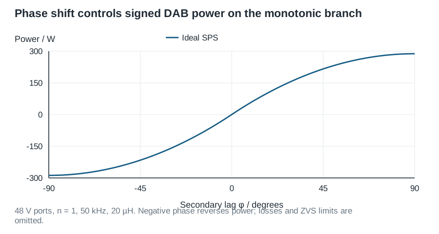
\[B-A=\frac{V_1\phi(\pi-\phi)}{\omega_sL_\sigma},\qquad \boxed{P=\frac{V_1V_2'}{\omega_sL_\sigma}\phi\left(1-\frac{\phi}{\pi}\right)}. \tag{8}\]Reversing the phase shift reverses the transfer direction. The signed extension is
\[P=\frac{nV_1V_2}{\omega_sL_\sigma}\phi\left(1-\frac{|\phi|}{\pi}\right), \qquad -\pi\leq\phi\leq\pi. \tag{9}\]The positive-power maximum occurs at \(\phi=\pi/2\); beyond it, increasing phase reduces power. Controllers normally select a monotonic branch. At zero phase with mismatched voltages, (5) predicts circulating AC current although (8) predicts zero average power. Zero transferred power therefore does not imply zero conduction loss in a real converter.
4. Calculate current stress
For a linear current segment with endpoints a and b, its mean square is \((a^2+ab+b^2)/3\). Applying this identity to both intervals gives
\[I_{\sigma,\mathrm{rms}}^2=\frac{1}{3\pi}\left[ \phi(I_0^2+I_0I_\phi+I_\phi^2) +(\pi-\phi)(I_\phi^2-I_\phi I_0+I_0^2)\right]. \tag{10}\]For \(V_1=V_2'\), the endpoints become \(I_0=-I_{\mathrm{pk}}\) and \(I_\phi=I_\pi=I_{\mathrm{pk}}\), where
\[I_{\mathrm{pk}}=\frac{V_1\phi}{\omega_sL_\sigma},\qquad \boxed{I_{\sigma,\mathrm{rms}}=I_{\mathrm{pk}}\sqrt{1-\frac{2\phi}{3\pi}}}. \tag{11}\]With 48 V ports, n = 1, 50 kHz and 20 µH, the 100 W low-angle operating point is
\[\Phi=0.3016767\ \mathrm{rad},\qquad I_{\mathrm{pk}}=2.30464\ \mathrm A,\qquad I_{\sigma,\mathrm{rms}}=2.22965\ \mathrm A. \tag{12}\]These are ideal transfer-current values. Magnetising current, dead time and parasitics require further analysis; device RMS currents also depend on conduction intervals.
5. Build a slow dynamic model
The ordinary cycle average of \(i_\sigma\) is zero for the chosen waveform, but the average of \(v_2'i_\sigma\) is generally nonzero. Replacing both switching quantities by their separate averages would discard the power-transfer mechanism.
Instead, assume that the DC voltages and phase change slowly compared with the switching period, and use the quasi-steady port power. For positive phase,
\[\bar i_2=\frac{P}{v_2} =\frac{nv_1}{\omega_sL_\sigma}\phi\left(1-\frac{\phi}{\pi}\right). \tag{13}\]This cancellation of \(v_2\) follows from the ideal SPS transfer law; it is not a universal property of isolated converters. For a standalone DAB feeding capacitor \(C_2\) and resistor R,
\[C_2\frac{dv_2}{dt}=\bar i_2-\frac{v_2}{R}. \tag{14}\]Here the output capacitor supplies the retained energy-storage state. Fast transfer-current transients have been eliminated by the quasi-steady approximation. The model is unsuitable for predicting individual switching transitions or rapid phase-command changes.
6. Perturb, substitute and linearise
Let \(v_1=V_1+\hat v_1\), \(v_2=V_2+\hat v_2\) and \(\phi=\Phi+\hat\phi\). The operating point satisfies
\[\frac{V_2}{R}=\frac{nV_1}{\omega_sL_\sigma}\Phi\left(1-\frac{\Phi}{\pi}\right). \tag{15}\]Expand (13) to first order, retaining terms proportional to one perturbation and discarding products such as \(\hat v_1\hat\phi\):
\[\hat i_2=K_\phi\hat\phi+K_{v1}\hat v_1, \qquad K_\phi=\frac{nV_1}{\omega_sL_\sigma}\left(1-\frac{2\Phi}{\pi}\right),\qquad K_{v1}=\frac{n}{\omega_sL_\sigma}\Phi\left(1-\frac{\Phi}{\pi}\right). \tag{16}\]Subtract (15) from the perturbed capacitor equation. With zero initial perturbations, the Laplace transform gives
\[(C_2s+1/R)\hat v_2=K_\phi\hat\phi+K_{v1}\hat v_1, \qquad G_{v\phi}(s)=\frac{K_\phi}{C_2s+1/R},\qquad G_{vv1}(s)=\frac{K_{v1}}{C_2s+1/R}. \tag{17}\]For the 100 W example, R = 23.04 Ω. With a standalone 470 µF capacitor, \(K_\phi=6.17226\ \mathrm{A/rad}\), \(K_{v1}=0.0434028\ \mathrm{A/V}\) and the pole is at \(s=-92.3463\ \mathrm{s}^{-1}\), or 14.6974 Hz. At \(\Phi=\pi/2\) the incremental phase gain vanishes, so this operating point provides no first-order phase control authority.
7. Change the load, change the plant
A downstream regulated converter can approximate a constant-power load over part of its control bandwidth. Replacing R by a load demanding \(P_\ell\) gives
\[C_2\dot v_2=\bar i_2-\frac{P_\ell}{v_2},\qquad \left(C_2s-\frac{P_\ell}{V_2^2}\right)\hat v_2 =K_\phi\hat\phi+K_{v1}\hat v_1-\frac{\hat p_\ell}{V_2}. \tag{18}\]The load draws more current when voltage falls. With fixed phase and a stiff primary source, this ideal model has an open-loop right-half-plane pole at \(P_\ell/(C_2V_2^2)\). It does not establish instability of a controlled SST: the actual load bandwidth, bus controller, parallel modules and source dynamics must be included.
The waveform power integrals were independently checked numerically at matched and mismatched voltages; the linearised coefficients were checked against finite-difference derivatives. These are analytical checks, not native simulator or hardware results. Return to the DAB tutorial for compensation and implementation. For a separate engineering example with design documentation, see TI’s TIDA-010054 DAB reference design.