
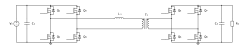
The dual-active-bridge (DAB) connects two DC ports through a switching-frequency transformer. Both ports use active full bridges, so the direction and magnitude of power transfer can be controlled. In our SST, each DAB connects one floating CHB DC link to the common low-voltage bus.
The transformer provides galvanic isolation and voltage scaling. A series inductance limits the rate of current change and participates in power transfer. It may consist of transformer leakage inductance, an external inductor, or both.
1. Define every reference before deriving power
Let \(V_1\) be the primary DC voltage and \(V_2\) the secondary DC voltage. Define
\[n=\frac{N_p}{N_s},\qquad V_2'=nV_2,\qquad L_\sigma=L_{\mathrm{leak},p}+n^2L_{\mathrm{leak},s}+L_{\mathrm{ext},p}. \tag{1}\]Include secondary external inductance with the same squared-ratio rule if present. Use an equivalent-circuit extraction that avoids counting leakage twice.
All following AC current and inductance quantities are primary-referred. Positive transfer current flows from the primary bridge towards the transformer. Positive transferred power flows from port 1 to port 2. The bridge outputs are \(v_1(t)\) and primary-referred \(v_2'(t)\).
For single-phase-shift (SPS) control, both full bridges generate symmetrical 50% duty square waves. Let the secondary waveform lag the primary by φ radians. Define \(\omega_s=2\pi f_s\) and, for the first derivation, \(0\leq\phi\leq\pi\).
2. Derive current from the voltage difference
Neglect magnetising current, losses, dead time and capacitor ripple initially. The transfer inductance obeys
\[L_\sigma\frac{di_\sigma}{dt}=v_1-v_2'. \tag{2}\]Set θ = \(\omega_st\). Over the first half cycle,
\[\frac{di_\sigma}{d\theta}=\begin{cases} (V_1+V_2')/(\omega_sL_\sigma),&0<\theta<\phi,\\ (V_1-V_2')/(\omega_sL_\sigma),&\phi<\theta<\pi. \end{cases} \tag{3}\]The second half cycle is the negative mirror for the symmetrical zero-DC-current solution. Thus \(i_\sigma(\pi)=-i_\sigma(0)\). This condition determines the endpoints; the companion derivation carries out that algebra and integrates the power.
The resulting ideal SPS transfer law is
\[\boxed{P=\frac{nV_1V_2}{\omega_sL_\sigma}\phi\left(1-\frac{|\phi|}{\pi}\right)},\qquad -\pi\leq\phi\leq\pi. \tag{4}\]| For negative phase shift, the sign of P reverses. We use the monotonic operating branch $$ | \phi | <\pi/2\(for the baseline controller. Positive-branch maximum ideal power occurs at\)\phi=\pi/2$$: |
This mathematical maximum is not a thermal or current rating.
3. Work the 100 W cell example
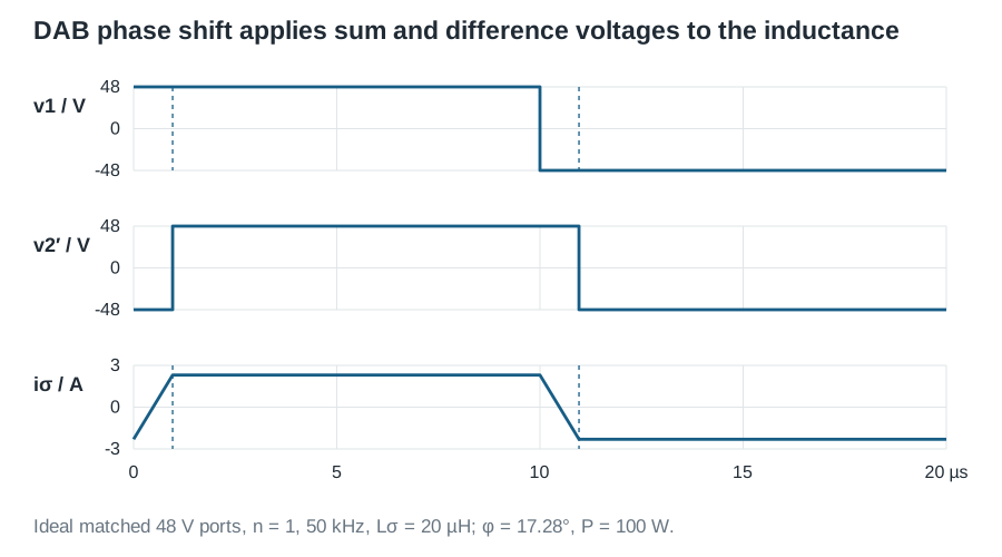
Use 48 V on both ports, n = 1, 50 kHz and 20 µH. Then \(P_{\max}=288\ \mathrm W\). Solving for the low-angle 100 W operating point gives
\[\Phi=\frac\pi2\left(1-\sqrt{1-P/P_{\max}}\right) =0.30168\ \mathrm{rad}=17.285^\circ. \tag{6}\]At matched voltages, current ramps from −2.305 A to +2.305 A during the phase interval and remains constant until the next commutation. The ideal average output current is \(P/V_2=2.083\ \mathrm A\).
For this matched case,
\[I_{\sigma,\mathrm{rms}}=I_{\mathrm{pk}}\sqrt{1-\frac{2\Phi}{3\pi}} \approx2.23\ \mathrm A. \tag{7}\]Average port current, transformer RMS current and semiconductor current are different quantities. Use the actual conduction intervals to determine device RMS current; add magnetising current and parasitic effects in the detailed model.
For a required power and selected phase range, the power expression can be rearranged to estimate L. Then check current stress over the complete voltage range. Choosing L solely to satisfy nominal power misses potentially large circulating current when \(V_1\neq nV_2\).
4. Why soft switching has an operating range
At a bridge transition, appropriately directed inductor current can charge and discharge switch-node capacitances before the next transistor turns on. If commutation completes during dead time, the incoming transistor can turn on at approximately zero drain-source voltage.
A preliminary energy comparison is
\[\frac12L_{\mathrm{comm}}I_{\mathrm{comm}}^2\gtrsim E_{\mathrm{cap,transition}}. \tag{8}\]This is only a screening condition. Current polarity, the commutation circuit, nonlinear output capacitance, magnetising current and available dead time also matter. A low average power does not guarantee enough commutation current. Confirm each bridge transition across the operating map using suitable device models and measured gate/switch-node timing. TI TIDA-010054 is an external example of a developed DAB reference design and its associated implementation resources.
SPS is a suitable first modulation method. Dual- and triple-phase-shift methods provide additional control variables for current shaping, but require their own interval analysis and constraints. Introduce them after the SPS baseline is verified.
5. Derive a useful low-frequency plant
The whole-period average of transformer AC current can be zero even while real power is transferred. Therefore replacing that AC current by its ordinary average loses the transfer mechanism. Begin instead with the cycle-averaged port power obtained from the switching waveforms.
For positive φ and a stiff primary source, the ideal secondary output current is
\[\bar i_2=\frac{P}{v_2} =\frac{nV_1}{\omega_sL_\sigma}\phi(1-\phi/\pi). \tag{9}\]For one standalone DAB supplying a resistor R and capacitor C2,
\[C_2\dot v_2=\bar i_2-v_2/R. \tag{10}\]Linearising at Φ gives
\[K_\phi=\frac{nV_1}{\omega_sL_\sigma}(1-2\Phi/\pi),\qquad \frac{\hat v_2}{\hat\phi}=\frac{K_\phi}{C_2s+1/R}. \tag{11}\]Here \(K_\phi\) has units A/rad. For the example it is 6.172 A/rad. With a 23.04 Ω load and 470 µF standalone test capacitor, the pole is approximately 14.7 Hz. This model assumes slow variation compared with a switching period and quasi-steady transfer waveforms. It does not resolve fast current transients or commutation; generalized averaging or sampled models can retain additional dynamics when needed.
The derivation page also includes input-voltage disturbance and explains why the damping changes for a constant-power load.
6. Design a standalone voltage controller
Let \(\hat\phi=G_c(s)(\hat v_2^*-\hat v_2)\) with \(G_c=K_p+K_i/s\). Under the preceding plant assumptions, the characteristic polynomial is
\[C_2s^2+(1/R+K_\phi K_p)s+K_\phi K_i. \tag{12}\]Matching a second-order target gives
\[K_p=\frac{2\zeta\omega_nC_2-1/R}{K_\phi},\qquad K_i=\frac{C_2\omega_n^2}{K_\phi}. \tag{13}\]For ζ = 0.707 and \(f_n=100\ \mathrm{Hz}\), the gains are approximately 0.0606 rad/V and 30.1 rad/(V·s). This is a continuous-time standalone example. Inspect the actual crossover, margins and delay effects; natural frequency is not automatically the loop crossover.
Bound phase shift within the selected monotonic branch, add anti-windup and use a current limit. At \(\Phi=\pi/2\) the incremental control gain vanishes. A voltage controller cannot be expected to maintain its designed dynamics near that limit.
7. Change the role when joining the SST bus
The standalone voltage controller is a commissioning exercise. In the assembled SST, one common-bus supervisor assigns output-current references to the six DABs. Each module can start with inverse-SPS feedforward, refined with measured current feedback and bounded differential sharing correction.
For a positive current command \(I_2^*\), the ideal inverse law is
\[\phi^*=\frac\pi2\left[1-\sqrt{1-\frac{4\omega_sL_\sigma I_2^*}{\pi nV_1}}\right]. \tag{14}\]The radicand must remain nonnegative, and practical current/phase limits are tighter than the algebraic limit. Use measured primary voltage and ramp references. The integral state of a standalone voltage loop must not remain active unnoticed after switching to current-command operation.
8. Build and validate the simulation
In PLECS, build two full bridges, a 1:1 ideal transformer and one explicit 20 µH primary-referred transfer inductance. Begin with stiff 48 V ports and a secondary source that can absorb power. Apply symmetrical 50% waveforms with 0.30168 rad lag. Integrate instantaneous port power over complete settled cycles.
Then replace the receiving source by a capacitor and resistor, add the voltage loop and compare the low-frequency response with the derived model. Introduce winding resistance, magnetising inductance, dead time and device capacitance one at a time. Changing several assumptions simultaneously makes discrepancies difficult to diagnose.
Use Simulink for the slow port-current model and sampled supervisory control. LTspice is useful for detailed commutation and gate-drive investigations. Native project files are not supplied in this draft; these are construction and verification instructions.
The transformer chapter turns voltage waveform and current stress into magnetic design constraints. PCB work must include both bridge commutation loops, local DC decoupling, current sensing, isolation boundaries and fault shutdown. The transfer inductor does not replace fast short-circuit protection.
9. Bench evidence to collect
Verify gate timing and transformer polarity at reduced voltage. Increase phase shift gradually under current-limited conditions. Compare measured voltage slopes and current endpoints with the piecewise model, then measure average power, RMS current and temperature. Test voltage-ratio mismatch before extrapolating an efficiency figure.
For each operating point, record which transitions achieve ZVS and which do not. A single clean waveform at rated power does not establish a full soft-switching range. Label every result as calculated, simulated or measured, with a model/board revision.