
A battery gives you 12 V, but your load needs 24 V. How can a circuit produce the higher voltage? How do you choose its components, keep the output steady, and turn a simulation into a board that works on the bench?
This tutorial follows one 12 V to 24 V, 30 W boost converter through that process. Start with the energy flow, build and test a model, design feedback, then move towards a physical prototype. The same example connects the circuit theory of an undergraduate course to control modelling and practical engineering.
First draft — design example, not a validated reference board. The numerical values below are analytical starting points. The accompanying MATLAB script and LTspice netlist are teaching resources; native simulator execution, completed PLECS/Simulink projects, a KiCad board and hardware measurements are not yet included. No efficiency or transient specification is claimed as a measured result.
Reading route: principles → design → open loop → models → feedback → implementation → simulation → PCB → bench → product.
If you already know the basic circuit and want the mathematics, open Small-Signal Modelling from First Principles: A Boost Converter Walkthrough. That companion article derives the model step by step rather than asking you to accept a transfer function without explanation.
1. What is a boost converter?
A boost converter is a switching DC–DC converter that raises an input voltage to a higher output voltage. The basic circuit uses an inductor, a controlled switch, a diode and an output capacitor. It is non-isolated: input and output share a ground connection. In this topology, there is no transformer.
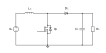
Here Q is normally a MOSFET. The diode anode faces the switching node; its cathode faces the output. C and the load are connected in parallel.
A higher voltage does not mean free energy. With efficiency defined as output power divided by input power,
\[\eta=\frac{P_{\mathrm{out}}}{P_{\mathrm{in}}},\qquad I_{\mathrm{in}}=\frac{V_{\mathrm{out}}I_{\mathrm{out}}}{\eta V_{\mathrm{in}}}. \tag{1}\]Delivering 30 W from 12 V requires 2.5 A at ideal efficiency, or about 2.78 A if efficiency is provisionally assumed to be 90%. That 90% is a sizing assumption, not a prediction.
The basic diode boost cannot regulate below its input voltage. It also has a path from input through the inductor and diode to the output even when Q is off. Disabling PWM therefore does not provide output isolation or necessarily interrupt an output short circuit.
Analysis conventions
Unless stated otherwise, the first calculations assume ideal components, continuous conduction, a resistive load and small switching ripple. Lowercase quantities denote time-varying values; uppercase quantities denote steady-state values; a hat denotes a small perturbation. The input voltage is \(v_g\), output voltage is \(v_o\) and inductor current is \(i_L\). L, C and R denote inductance, output capacitance and load resistance.
Watch one switching cycle
Let the switching period be \(T_s=1/f_s\). Duty ratio \(d\) is the fraction of each period for which Q conducts; its steady-state value is \(D\).
Q on, diode off: the input is applied across the inductor. Its current rises, while the output capacitor supplies the load. For ideal components,
\[L\frac{di_L}{dt}=v_g,\qquad C\frac{dv_o}{dt}=-\frac{v_o}{R}. \tag{2}\]Q off, diode on: the inductor current continues through the diode into the output. The input and inductor together deliver energy to the output. Assuming the output exceeds the input,
\[L\frac{di_L}{dt}=v_g-v_o,\qquad C\frac{dv_o}{dt}=i_L-\frac{v_o}{R}. \tag{3}\]An inductor obeys \(v_L=L\,di_L/dt\), so its current cannot change instantaneously under a finite voltage. This continuity is the reason it can keep delivering current when the switch opens. Its stored energy is \(E_L=Li_L^2/2\).
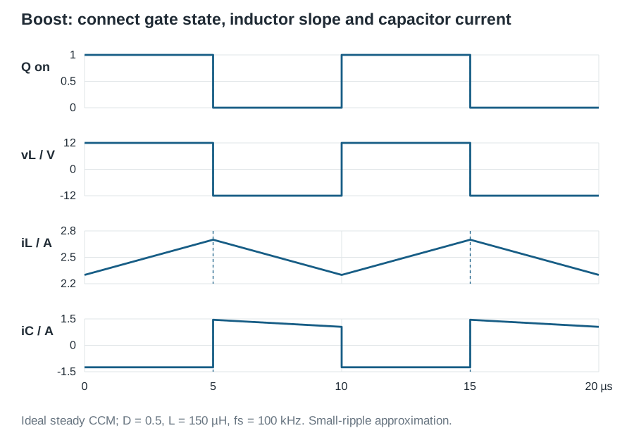
Explore it: change duty ratio and follow one switching cycle
This recalculates an ideal CCM steady state at each duty ratio. It is not a startup or transient simulation. Input voltage, resistance, L = 150 µH and fs = 100 kHz stay fixed.
At D = 0.50: 12 V → 24 V, R = 19.2 Ω. Inductor current = 2.50 A; ripple = 0.40 A peak-to-peak.
The current axis follows the calculated minimum and maximum; compare the numeric ripple values as well as the shape.
Q on: input → L → Q → return. The output diode blocks, so the output capacitor supplies the load while inductor current rises.
Derive the conversion ratio
In periodic steady state, the energy-storage states repeat after each switching period. Integrating the inductor and capacitor laws gives inductor volt-second balance and capacitor charge balance:
\[\int_0^{T_s}v_L(t)\,dt=0,\qquad \int_0^{T_s}i_C(t)\,dt=0. \tag{4}\]With small ripple in continuous conduction mode, the first balance becomes
\[D V_g+(1-D)(V_g-V)=0, \tag{5}\]which gives
\[\boxed{V=\frac{V_g}{1-D}},\qquad \boxed{D=1-\frac{V_g}{V}}. \tag{6}\]The average capacitor current is also zero:
\[(1-D)I_L=\frac{V}{R}=I_o. \tag{7}\]At 12 V input and 24 V output, the ideal duty is 0.5. These relations describe the ideal CCM steady state; parasitic losses and discontinuous conduction change the result. Increasing duty towards one is not a route to unlimited real output voltage.
CCM and DCM
In continuous conduction mode (CCM) the inductor current stays above zero. In discontinuous conduction mode (DCM) it falls to zero and remains there for part of the switching period. DCM introduces a third interval in which both the switch and diode are off.
The CCM equations below cannot simply be extended into DCM. At light load, observe the inductor current and change the model if the operating mode changes.
2. Turn a requirement into component values
Before selecting parts, write down the operating envelope. Here is the provisional specification for our teaching example.
| Quantity | Starting value or objective |
|---|---|
| Input voltage | 12 V nominal; 10–14 V design range |
| Output voltage | 24 V |
| Maximum output power | 30 W |
| Rated output current | 1.25 A |
| Nominal resistive load | 19.2 Ω |
| Switching frequency | 100 kHz |
| Inductor | 150 µH starting value |
| Output capacitance | 330 µF effective starting value |
| Steady switching-ripple objective | Below 240 mV peak-to-peak; to be verified |
| Topology | Single-phase, diode-rectified boost |
The effective capacitance means the value available in operation, including tolerance and any voltage dependence. Transient voltage excursion is a separate requirement from switching ripple; we will establish it when choosing the control bandwidth and load-step specification.
Size the inductor
The on-state current rise gives the approximate peak-to-peak ripple:
\[\Delta i_{L,\mathrm{pp}}=\frac{V_gD}{Lf_s}. \tag{8}\]At the nominal operating point, choosing 150 µH gives
\[\Delta i_{L,\mathrm{pp}}= \frac{12\times0.5}{150\times10^{-6}\times100\times10^3} =0.40\ \mathrm{A}. \tag{9}\]The ideal average input and inductor current is 2.5 A, so
\[I_{L,\mathrm{pk}}\approx I_L+\frac{\Delta i_{L,\mathrm{pp}}}{2}=2.70\ \mathrm{A}, \tag{10}\] \[I_{L,\mathrm{rms}}\approx\sqrt{I_L^2+\frac{\Delta i_{L,\mathrm{pp}}^2}{12}}. \tag{11}\]Check the whole input range. At 10 V, using the provisional 90% efficiency assumption gives 3.33 A average input current. Using ideal duty 0.583 as a first ripple estimate gives about 0.389 A ripple and 3.53 A peak. This mixed ideal/loss estimate is only for preliminary sizing; a lossy model must determine the actual duty and current.
Choose saturation and thermal current ratings with allowance for tolerance, temperature, startup and the intended current limit. A part rated only for the nominal 2.70 A peak leaves too little information to make that decision.
The ideal CCM boundary occurs at \(I_L=\Delta i_{L,\mathrm{pp}}/2\). At nominal duty,
\[I_{o,\mathrm{boundary}}\approx(1-D)\frac{\Delta i_{L,\mathrm{pp}}}{2} =0.10\ \mathrm{A}. \tag{12}\]This is about 2.4 W at 24 V. The nominal CCM model therefore needs reconsideration near that light-load region.
Size the capacitor
During the on interval the output capacitor supplies the load. Neglecting ESR and assuming small ripple,
\[\Delta v_{o,\mathrm{pp}}\approx\frac{I_oD}{Cf_s}. \tag{13}\]For 330 µF at the nominal point, this is approximately 18.9 mV. This is the capacitive switching-ripple component only. ESR, ESL, diode commutation and PCB inductance add to the measured waveform.
Neglecting inductor ripple, capacitor RMS current is approximately
\[I_{C,\mathrm{rms}}\approx I_o\sqrt{\frac{D}{1-D}}, \tag{14}\]or 1.25 A here. Check ripple-current capability as well as capacitance and voltage rating.
For a sudden increase in load, the capacitor initially supplies the current deficit:
\[\Delta v_o(t)\approx-\frac{1}{C}\int_0^t\Delta i_{\mathrm{deficit}}(\tau)\,d\tau. \tag{15}\]This explains why a small calculated switching ripple does not guarantee a small load-transient dip.
Select devices and estimate losses
In the ideal circuit, MOSFET off-state voltage and diode reverse voltage are approximately the output voltage. Real devices must also tolerate overshoot and operating extremes. Check MOSFET conduction and switching losses, gate-drive requirements, diode forward loss and recovery, and inductor copper and core losses.
Useful first estimates are
\[P_{Q,\mathrm{cond}}\approx D\left(I_L^2+\frac{\Delta i_L^2}{12}\right)R_{\mathrm{DS(on)}}, \qquad P_D\approx V_F I_o, \tag{16}\] \[P_{Q,\mathrm{sw}}\approx\frac12 V_{\mathrm{DS}}I_{\mathrm{sw}}(t_r+t_f)f_s, \qquad P_{L,\mathrm{Cu}}=I_{L,\mathrm{rms}}^2r_L. \tag{17}\]The switching-loss expression is a rough overlap estimate, not a substitute for device waveforms or characterised switching energy. Temperature changes the parameters, and core loss requires a suitable magnetic model. TI’s power-stage calculation note provides a useful independent component-sizing reference.
3. Build an open-loop simulation first
Connect the source, inductor, switch, diode, capacitor and resistor. Set a 100 kHz PWM signal with duty 0.5. Plot inductor current, switch-node voltage and output voltage.
After startup, an ideal CCM circuit should approach 24 V with about 2.5 A average inductor current and 0.40 A ripple. A model containing voltage drops and resistance will differ. Record the cause rather than forcing every model to match the ideal calculation.
Next change input voltage while keeping duty fixed. The ideal gain predicts 20 V output at 10 V input and 28 V at 14 V input. That is the first reason to add feedback.
Then vary load. In an ideal CCM model the DC voltage gain is independent of R, although the transient and current change. In a real converter, losses cause load-dependent output error; at sufficiently light load, DCM also changes the gain. Distinguishing these effects is a useful modelling exercise.
Do not mistake a steady-state model for a startup model. Starting the capacitor at zero can involve diode conduction and inrush that the two-interval CCM average model does not capture correctly. Use a switching model for startup and protection behaviour.
4. Choose the right mathematical model
Each model answers a different question.
| Model | What it retains | What to use it for |
|---|---|---|
| Switching model | Individual on/off intervals | Ripple, device stress, startup and switching events |
| Nonlinear averaged model | Cycle-averaged energy flow | Slower trajectories while its conduction assumptions remain valid |
| Linear small-signal model | First-order changes around one operating point | Transfer functions, Bode plots and local feedback design |
| Sampled/discrete control model | Sampling, update timing and delay | Digital implementation and its additional stability limits |
For the ideal CCM converter with a resistive load, the averaged equations are
\[L\frac{di_L}{dt}=v_g-(1-d)v_o, \qquad C\frac{dv_o}{dt}=(1-d)i_L-\frac{v_o}{R}. \tag{18}\]Here the variables represent cycle averages. The equations are still nonlinear because duty multiplies voltage and current. Averaging and linearisation are two different operations.
Write each variable as its operating point plus a small perturbation, such as \(d=D+\hat d\) and \(v_o=V+\hat v_o\). Removing the equilibrium terms and neglecting products of perturbations yields
\[L\frac{d\hat i_L}{dt}=\hat v_g-(1-D)\hat v_o+V\hat d, \tag{19}\] \[C\frac{d\hat v_o}{dt}=(1-D)\hat i_L-I_L\hat d-\frac{\hat v_o}{R}. \tag{20}\]Holding input voltage fixed, the duty-to-output transfer function is
\[\boxed{G_{vd}(s)=\frac{\hat v_o(s)}{\hat d(s)} =\frac{(1-D)V-LI_Ls}{LCs^2+(L/R)s+(1-D)^2}}. \tag{21}\]The companion tutorial explains why perturbations are introduced, exactly which terms are discarded, and how this fraction is derived. It also derives the line-to-output response and output impedance.
The boost converter’s right-half-plane zero
Define the complementary duty ratio \(D'=1-D\); write \(q=D'\) for compactness. The natural frequency, quality factor and right-half-plane zero are
\[\omega_0=\frac{q}{\sqrt{LC}},\qquad Q=Rq\sqrt{\frac{C}{L}},\qquad \omega_{z,\mathrm{RHP}}=\frac{Rq^2}{L}. \tag{22}\]For this example, \(f_0\approx358\ \mathrm{Hz}\), \(Q\approx14.24\) and \(f_{z,\mathrm{RHP}}\approx5.09\ \mathrm{kHz}\). Frequencies in hertz are angular frequencies divided by \(2\pi\).
Increasing duty initially shortens the time during which the inductor feeds the output. The capacitor can therefore begin to discharge faster, even though the eventual output voltage rises. The model captures this inverse response with the numerator factor \(1-s/\omega_{z,\mathrm{RHP}}\).
This zero adds phase lag and constrains useful bandwidth. It cannot be safely cancelled by placing an unstable pole in the controller. Its frequency also changes with load and operating point. Analog Devices AN-149 discusses the boost power stage and this control limitation.
5. Close the feedback loop deliberately
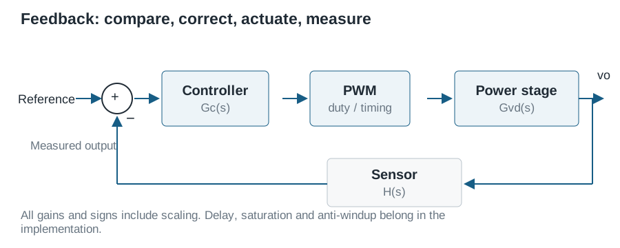
Start with voltage-mode control: measure output voltage, compare it with a reference, and use a compensator to adjust duty. The small-signal loop gain is
\[T(s)=G_c(s)G_{\mathrm{PWM}}(s)G_{vd}(s)H(s), \tag{23}\]where \(H\) is the sensing path and \(G_{\mathrm{PWM}}\) converts the controller output to duty. For an analogue ramp of peak-to-peak amplitude \(V_{\mathrm{ramp}}\), its low-frequency gain is approximately \(1/V_{\mathrm{ramp}}\). For a controller expressed directly in duty units, it is one before adding timing effects.
With negative feedback, the reference-to-output response is
\[\frac{\hat v_o}{\hat v_{\mathrm{ref}}} =\frac{G_cG_{\mathrm{PWM}}G_{vd}}{1+T}. \tag{24}\]This reference is expressed in the same units as the sensed feedback. Rescaling the measurement changes the controller gains.
A reproducible, intentionally slow first controller
For a teaching baseline, let the software reconstruct output voltage in volts, so \(H=1\), and let the controller produce duty directly. Choose a PI controller:
\[G_c(s)=K_p+\frac{K_i}{s},\qquad K_p=2.0\times10^{-4}\ \mathrm{V}^{-1},\quad K_i=0.65\ \mathrm{V}^{-1}\mathrm{s}^{-1}. \tag{25}\]Its nominal crossover is about 5 Hz. This is intentionally slow: the lossless plant has a strong resonance near 358 Hz, and simply pushing a PI crossover upwards can create additional unity-gain crossings. This controller demonstrates regulation; it is not offered as a production transient-performance design.
The MATLAB analysis script builds the plant and controller, lists all stability margins and plots the small-signal responses. It requires MATLAB with Control System Toolbox. The supplied values and continuous-time stability have been independently checked numerically; the script has not yet been run in MATLAB.
Move from the baseline to a useful design
- Evaluate the plant over the input range, load range and component tolerances, keeping track of CCM/DCM boundaries.
- Set transient-response objectives, then choose a candidate crossover well below switching frequency and the lowest relevant RHP-zero frequency. For an initial study, \(f_c<\min(f_s/10,f_{z,\mathrm{RHP,min}}/10)\) is a conservative starting constraint, not proof of stability.
- Select PI, Type II or Type III compensation according to the actual plant phase and the required bandwidth. A PI that works at very low frequency may be inadequate near or above the LC resonance.
- Include sensing filters, PWM gain, delay and parasitics. Inspect every gain crossing and the closed-loop poles, not only one displayed phase margin.
- Aim initially for at least 60° phase margin and 10 dB gain margin across the specified CCM operating points; treat these as design objectives to be verified.
- Check line steps, load steps, startup, duty saturation and recovery in the switching model. Establish a separate light-load strategy when DCM is involved.
A generic Type III form is
\[G_c(s)=K\frac{(1+s/\omega_{z1})(1+s/\omega_{z2})} {s(1+s/\omega_{p1})(1+s/\omega_{p2})}. \tag{26}\]Do not place its poles and zeros by copying another converter’s component values. They must work with this converter’s measured or modelled plant.
Current-mode control adds an inner current loop. That can simplify the outer-loop behaviour, but it changes the plant seen by the voltage controller. Peak current-mode implementations also need slope-compensation and sampled-current analysis where appropriate; the duty-to-voltage model above alone does not certify their stability.
6. Implement the controller: analogue or digital
These are two implementation routes built on the same power stage and feedback principles.
Analogue route
A reference, output divider, error amplifier, compensation network, PWM comparator and gate driver form a basic voltage-mode implementation. A controller IC can integrate several of these blocks.
For a divider,
\[V_{\mathrm{fb}}=V_o\frac{R_{\mathrm{bottom}}}{R_{\mathrm{top}}+R_{\mathrm{bottom}}}. \tag{27}\]A 2.4 V reference at 24 V output requires a nominal 0.1 sensing gain. Include this gain and the PWM ramp amplitude when translating a compensator into actual resistors and capacitors. The direct-duty PI numbers above cannot be pasted into an error-amplifier circuit without that scaling.
Use LTspice first with behavioural blocks, then with a suitable amplifier or controller model. Add output swing limits, supply rails and the gate driver. A linear compensator that asks its amplifier for an impossible voltage will not behave as the algebra predicts.
Digital route
A microcontroller or DSP samples voltage with an ADC, computes a control action and updates a PWM peripheral. Set the sampling period to \(T_a\), which is distinct from the switching period even if both are 10 µs in the first example.
For the PI above, Tustin discretisation uses
\[\frac1s\approx\frac{T_a}{2}\frac{1+z^{-1}}{1-z^{-1}}. \tag{28}\]The unsaturated incremental controller becomes
\[u[k]=u[k-1]+\left(K_p+\frac{K_iT_a}{2}\right)e[k] +\left(-K_p+\frac{K_iT_a}{2}\right)e[k-1]. \tag{29}\]Here \(u\) is the duty correction, and \(e\) is output-voltage error in volts. At \(T_a=10\ \mu\mathrm{s}\), the two error coefficients are 0.00020325 and −0.00019675.
Add an operating duty bias or feedforward term and enforce bounds:
\[d[k]=\operatorname{clip}\bigl(D_{\mathrm{ff}}[k]+u[k],d_{\min},d_{\max}\bigr), \qquad D_{\mathrm{ff}}\approx1-\frac{v_g}{V_{\mathrm{target}}}. \tag{30}\]The feedforward expression is for a valid positive target above the input, not a startup law. Choose duty limits from the actual hardware. Add anti-windup so the integrator does not keep accumulating error while duty is limited; a separate integrator state with conditional integration or back-calculation makes this explicit. The incremental equation by itself has no anti-windup.
Account for ADC scaling, quantisation, PWM resolution, sample timing, computation time and when a new duty actually takes effect. An effective delay contributes approximately
\[G_{\mathrm{delay}}(s)=e^{-sT_d},\qquad \phi_{\mathrm{delay}}(\omega)=-\omega T_d. \tag{31}\]Use a sampled-data model for the final digital stability check. Firmware must also define startup, shutdown, soft-start, fault handling and recovery. Fast overcurrent protection should not depend only on a slow voltage-regulation loop.
7. Keep the simulations comparable
Use the same parameter names, operating points and test events across tools.
| Environment | Suggested exercise | Current draft resource |
|---|---|---|
| PLECS | Ideal switched stage, averaged stage, then continuous and sampled control | Construction recipe below; native project pending |
| MATLAB/Simulink | Transfer functions, sampled PI, closed-loop system simulation | MATLAB analysis script supplied; native Simulink model pending |
| LTspice | Switching waveforms, then analogue compensation and device models | Open-loop starter netlist supplied; native execution pending |
LTspice is available free from Analog Devices, making it a useful accessible route for the circuit-level exercises. Access to PLECS and MATLAB/Simulink depends on the reader’s licences.
Construct the PLECS or Simulink models
For the switched model, use a DC source, 150 µH inductor, switch, diode, 330 µF capacitor and 19.2 Ω resistor. Drive the switch with a 100 kHz pulse generator and observe the three waveforms listed earlier. Use switching-capable solver settings and repeat with a smaller step or tighter tolerance to check convergence.
For the averaged model, implement the two averaged derivatives with two integrators. Initialise them at 2.5 A and 24 V for local perturbation experiments. Close the loop with the PI, a duty limiter and an explicit anti-windup implementation. For digital control, add a zero-order-held measurement, a discrete controller and the intended PWM-update delay.
Do not use the averaged model to claim switching ripple: averaging has deliberately removed it.
Open the LTspice starter
Download boost_open_loop.cir and open it in LTspice. It uses a voltage-controlled switch, a simple diode and illustrative winding resistance, so the output will not be exactly the ideal 24 V. These are generic parts, not a selected production BOM.
Run its transient analysis and plot V(out), V(sw) and I(L1). Compare the last few switching periods with the earlier calculations. The file starts from an input-connected operating point and then applies PWM; it is not a simulation of connecting a battery to a fully discharged board. Increase the simulation duration if the waveform has not settled.
Use a shared test sheet
At minimum, compare nominal operation, 10 V and 14 V input, half and full load, a half-to-full-load step, startup, duty limiting and light load near the CCM boundary. Separate small perturbations used for model validation from large events used to test nonlinear behaviour.
Record the simulator/version, component-model assumptions, timestep settings, steady output, ripple, peak current and transient recovery. Leave efficiency blank in an ideal model, or label its ideal result explicitly; useful loss estimates require lossy component models.
8. Move into KiCad and PCB design
The circuit diagram is only part of the hardware design. Before layout, add the gate driver, local input decoupling, voltage and current sensing, protection, connector ratings and test points. Select real parts and check their footprints against manufacturer drawings.
A practical KiCad workflow is:
- Capture the complete schematic and annotate component values and ratings.
- Assign verified footprints and run electrical rules checks.
- Place the switching devices and output decoupling to keep the high-frequency commutation loop short. In a diode boost, pay particular attention to the switch–diode–output-capacitor loop.
- Keep the switching node compact, route the gate-drive return closely, and keep sensitive feedback away from switching edges. Use Kelvin sensing where needed and plan return-current paths.
- Size copper for current and temperature rise, then check clearances, thermal paths and manufacturability.
- Run design rules checks and inspect the board before generating Gerbers, drill files, BOM and assembly data.
Automation can help generate repetitive schematic content and organise layout. Electrical and design rules checks do not prove low EMI, correct loop compensation or adequate cooling. Those require engineering review and measurements.
A future downloadable KiCad project should identify its board revision and match the tested BOM. This draft does not yet include a routed or tested PCB.
9. Bring up the prototype and compare it with the model
Begin with visual inspection, polarity and continuity checks. Verify auxiliary rails, controller operation and PWM timing before sustained power conversion. Use a current-limited source and a defined load for staged power-up; choose the current limit and ramp procedure from the component limits.
Remember the input-to-output diode path. PWM off does not mean the output capacitor is uncharged. Check probe grounding and voltage ratings before measuring the switching node, and discharge stored energy before handling the board.
Record:
- Output regulation over input and load range.
- Switching ripple with a documented probe connection and measurement bandwidth.
- Inductor current and switch-node stress, including startup and load changes.
- Input/output power at defined electrical boundaries, with instrument uncertainty.
- Temperatures after reaching an identified thermal condition.
- Line/load transients, limiting behaviour and recovery from intended fault tests.
Measured efficiency is
\[\eta=\frac{\langle v_o(t)i_o(t)\rangle}{\langle v_g(t)i_g(t)\rangle}. \tag{32}\]For sufficiently steady DC rails, products of DC readings may approximate these average powers. Include auxiliary supplies consistently and state what is included.
If the measurement disagrees with simulation, investigate the assumptions: effective capacitance, inductor DCR and saturation, diode drop, switching loss, sensor filtering, timing and layout parasitics. Update the model and repeat the test. That feedback is part of the converter’s development process.
10. A working prototype is a milestone towards a product
A board that regulates at one operating point is a useful achievement. Turning it into a dependable product adds repeatability across component tolerances, temperature, production units, supply conditions and load behaviour.
The next work includes thermal design, EMI and EMC evaluation, protection coordination, reliability, sourcing, assembly and production testing. Applicable requirements depend on the end application; this teaching example does not establish product compliance.
Once the basic converter is understood, extensions include synchronous rectification, interleaving, current-mode control, better magnetics and application-specific optimisation. Each introduces new trade-offs and, often, new models.
The central habit remains the same: write down the requirement, explain the energy flow, calculate, simulate, build, measure and revise. A model is valuable because it helps you make and test a design decision.
Continue with the derivation: Small-Signal Modelling from First Principles: A Boost Converter Walkthrough.
Further study
Robert W. Erickson and Dragan Maksimović, Fundamentals of Power Electronics, third edition, Springer, 2020. Relevant chapters cover steady-state converter analysis, AC equivalent circuit modelling, converter transfer functions and controller design. The derivations and numerical example on this page are presented independently; this article is not a reproduction of the textbook.