
In hard switching, transistor voltage and current overlap during a transition. The resulting energy per event contributes to loss as switching frequency increases. Earlier chapters also introduced ways of achieving soft switching; the LLC makes a resonant network central to the conversion process.
The LLC resonant converter uses a resonant current to commutate switch capacitances during dead time. When the current has the right direction and sufficient charge-transfer capability, the next MOSFET can turn on at near-zero drain–source voltage. This reduces turn-on loss, but does not remove turn-off, conduction, magnetic or drive losses. ZVS must be demonstrated over the intended operating range.
The baseline studied here regulates by switching frequency while maintaining approximately 50% complementary drive. The gain is therefore a function of frequency, load and the tank parameters.
This article works through a 390 V to 12 V, 240 W LLC — the canonical application, converting a PFC output bus to a low-voltage rail.
First draft — design example, not a validated reference board. Values are analytical starting points. The FHA model below is a sizing tool, not a certification; verify with a switching simulation. Native simulator execution and hardware measurements are not included.
Reading route: why resonance → the tank → gain curves → ZVS → design → light load → control → simulation → applications.
1. Why resonance
In a hard-switched converter the switch current and voltage overlap during every transition, dissipating roughly
\[P_{\mathrm{sw}}\approx\tfrac12V_{\mathrm{DS}}I_{\mathrm{sw}}(t_r+t_f)f_s. \tag{1}\]Equation (1) is a rough linear-overlap estimate. Transition times, capacitances and current depend on the device and gate circuit, so they are not fixed application constants. Frequency increases can reduce a required volt-second product, but magnetic volume does not generally scale as exactly 1/fs once loss and temperature are included.
A resonant converter attacks the \(V_{\mathrm{DS}}I_{\mathrm{sw}}\) product directly. Instead of chopping a voltage into a rectangular wave and filtering it, it drives a resonant tank whose current is nearly sinusoidal and lags the applied voltage. If the current still flows in the right direction when a switch turns off, that current will discharge the incoming switch’s capacitance during the dead time — so the next device turns on at essentially zero volts.
That is zero-voltage switching (ZVS) at turn-on. The turn-on overlap term can become small; turn-off loss and the other loss mechanisms remain. Light load, startup and voltage extremes require separate commutation checks.
2. The tank: three elements, two resonances
The name describes the tank: two inductances and a capacitance, L–L–C.

- \(L_r\) — the series resonant inductance (often just the transformer’s leakage inductance).
- \(C_r\) — the series resonant capacitor, which blocks steady DC current but does not eliminate startup, imbalance or transient flux checks.
- \(L_m\) — the transformer’s magnetising inductance, deliberately made small so that it participates in the resonance instead of being a parasitic nuisance.
Magnetising inductance is an intentional tank parameter. It contributes circulating current and influences both gain and commutation. An external resonant inductor can provide Lr while the transformer has tight coupling; alternatively, part of Lr can be realised as designed leakage. An LLC transformer is not inherently a poorly coupled transformer.
The two resonances are:
\[f_r=\frac{1}{2\pi\sqrt{L_rC_r}} \qquad\text{(series resonance, with the output loaded)} \tag{2}\] \[f_m=\frac{1}{2\pi\sqrt{(L_r+L_m)C_r}} \qquad\text{(lower resonance, output unloaded)} \tag{3}\]During secondary conduction, the rectifier approximately clamps the transformer voltage. Magnetising current continues to change under that voltage; Lm is not literally short-circuited. When the rectifier is off, a different resonant interval results. The two frequencies identify useful limiting behaviours; the loaded converter needs the complete equivalent circuit.
For our example, with \(L_r=80\ \mu\mathrm{H}\), \(C_r=33\ \mathrm{nF}\) and \(L_m=400\ \mu\mathrm{H}\):
\[f_r=97.95\ \mathrm{kHz},\qquad f_m=39.99\ \mathrm{kHz}. \tag{4}\]The two design ratios
Everything about an LLC’s character is captured by two dimensionless numbers:
\[L_n=\frac{L_m}{L_r}, \qquad Q=\frac{\sqrt{L_r/C_r}}{R_{ac}}, \qquad R_{ac}=\frac{8}{\pi^2}n^2R_{\mathrm{load}}. \tag{5}\]\(L_n\) is the inductance ratio — small values give more gain range but more circulating current. \(Q\) is the loaded quality factor, and because \(R_{ac}\) depends on the load, \(Q\) changes with load: light load means low \(Q\), full load means high \(Q\). The factor \(8/\pi^2\) converts the square-wave-driven rectifier and load into the equivalent resistance seen by the fundamental.
For our design: \(L_n=5.0\), \(R_{ac}=124.5\ \Omega\) and \(Q=0.396\) at full load.
3. The gain curve — the LLC’s central design tool
Assume only the fundamental of the square-wave excitation transfers power. This first harmonic approximation (FHA) gives the tank’s voltage gain as a function of normalised frequency \(f_n=f_s/f_r\):
\[\boxed{M(f_n)=\cfrac{1}{\sqrt{\left(1+\cfrac{1}{L_n}-\cfrac{1}{L_nf_n^2}\right)^2+Q^2\left(f_n-\cfrac{1}{f_n}\right)^2}}} \tag{6}\]and the output follows from the half-bridge excitation and the turns ratio:
\[V_{\mathrm{out}}=M\cdot\frac{V_{\mathrm{in}}/2}{n}. \tag{7}\]Evaluating (6) at \(L_n=5\) across load:
| \(f_n\) | Q=0.1 (light) | Q=0.2 | Q=0.396 (full) | Q=0.8 (overload) |
|---|---|---|---|---|
| 0.50 | 2.341 | 2.000 | 1.396 | 0.791 |
| 0.60 | 1.531 | 1.473 | 1.298 | 0.935 |
| 0.70 | 1.258 | 1.242 | 1.187 | 1.017 |
| 0.80 | 1.125 | 1.121 | 1.105 | 1.044 |
| 0.90 | 1.049 | 1.048 | 1.045 | 1.033 |
| 1.00 | 1.000 | 1.000 | 1.000 | 1.000 |
| 1.10 | 0.966 | 0.966 | 0.964 | 0.956 |
| 1.20 | 0.942 | 0.940 | 0.934 | 0.908 |
| 1.40 | 0.909 | 0.904 | 0.884 | 0.815 |
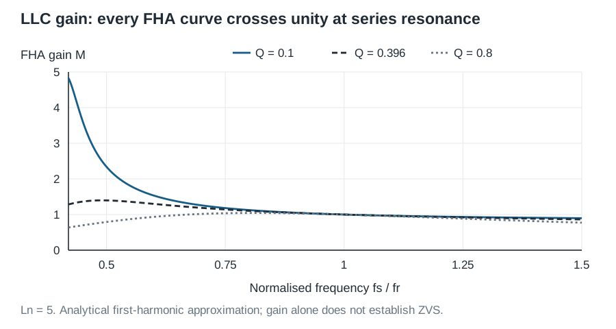
Read three things from this table
One. At fs = fr, the series Lr and Cr reactances cancel, so the FHA voltage-divider gain is unity at every finite load represented by this model. The input still sees Lm in parallel with the referred load: it is not generally purely resistive. Unity gain is a useful design anchor, not proof of maximum efficiency or ZVS.
Two. Above \(f_n=1\) the gain is below 1 and only mildly load-dependent — a gentle, well-behaved buck region.
Three. Below resonance the gain can exceed unity, then turns over as frequency is reduced further. The load moves both the gain peak and the input-reactance boundary. Some sub-resonant points have gain below unity, as the table shows.
For our design, choosing \(n=16\) puts the output at \(M=1\) at
\[V_{\mathrm{out}}=\frac{390/2}{16}=12.19\ \mathrm{V}, \tag{8}\]so the converter runs just above resonance to trim to 12.0 V — an ideal operating point.
Peak gain sets the hold-up capability
At full load (\(Q=0.396\)) the gain peaks at
\[M_{\mathrm{peak}}\approx1.398\quad\text{at}\quad f_n\approx0.491\ (48.1\ \mathrm{kHz}). \tag{9}\]If only the unconstrained FHA gain magnitude were considered, the formal minimum input voltage would be
\[V_{\mathrm{in,min}}=\frac{2nV_{\mathrm{out}}}{M_{\mathrm{peak}}}=274.7\ \mathrm{V}. \tag{10}\]This formal value is not an established hold-up limit. The gain peak can lie in the capacitive region, so that operating point may be unusable. The next section checks input reactance independently. Hold-up time also depends on the usable DC-link capacitor energy, load and losses, even after an acceptable minimum bus voltage has been established.
4. Check the inductive region and the commutation charge
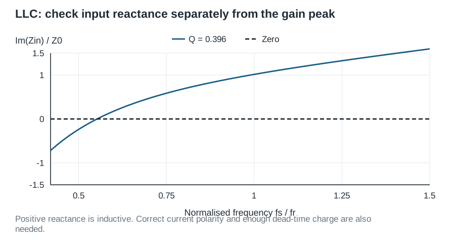
The FHA gain peak describes a voltage ratio. The sign of input reactance answers a different question: does the fundamental current lag or lead the drive voltage? Derive the latter from the same equivalent circuit. With Z0 = √(Lr/Cr), Ln = Lm/Lr, Q = Z0/Rac and x = fs/fr,
\[\frac{\operatorname{Im}Z_{\mathrm{in}}}{Z_0} =x-\frac1x+\frac{xL_n}{1+(xL_nQ)^2}. \tag{11a}\]The first two terms are the series Lr–Cr reactance. The last is the imaginary part of the parallel Lm–Rac branch. Positive input reactance is inductive; zero marks the FHA boundary. It is not generally located at the maximum of the gain-magnitude curve.
For Ln = 5 and Q = 0.396, the boundary is about x = 0.5525, or 54.1 kHz. The unconstrained gain peak is near x = 0.491 and lies on the capacitive side. At the boundary the gain is approximately 1.355; practical operation needs inductive and commutation margin beyond that mathematical boundary.
Inductive input impedance is useful but insufficient evidence of ZVS. During each dead time, current must transfer enough charge to move the switch node to the intended rail before turn-on. A screening condition is
\[\left|\int_{\mathrm{dead\ time}} i_{\mathrm{comm}}(t)\,dt\right| \gtrsim Q_{\mathrm{oss,upper}}(V_{\mathrm{in}}) +Q_{\mathrm{oss,lower}}(V_{\mathrm{in}})+Q_{\mathrm{stray}}, \tag{11b}\]| with the current flowing in the required direction. For identical constant capacitances and approximately constant current, this reduces to | Icomm | tdead ≳ 2 Coss Vin. Real Coss is nonlinear; the incoming MOSFET voltage at its actual gate turn-on is the decisive waveform check. TI’s LLC design seminar discusses the separate inductive-region and commutation-energy requirements. |
A frequency limit must cover load, line, tolerances, startup and faults. Starting at high frequency and ramping towards regulation is a common strategy, but its limits still require analysis; a single nominal gain curve cannot define a safe operating envelope.
5. Designing the tank
| Quantity | Value |
|---|---|
| Input | 390 V nominal (PFC output) |
| Output | 12 V, 20 A, 240 W (0.6 Ω) |
| Turns ratio \(n\) | 16 |
| \(L_r\) | 80 µH |
| \(C_r\) | 33 nF |
| \(L_m\) | 400 µH (\(L_n=5\)) |
| \(f_r\) | 97.95 kHz |
A workable sequence:
- Choose \(n\) so that \(M=1\) at nominal input: \(n=V_{\mathrm{in,nom}}/(2V_{\mathrm{out}})\). This places the nominal point near unity FHA gain; evaluate efficiency separately.
- Choose \(L_n\) — typically 3 to 8. Lower gives more gain range and better hold-up but more circulating current and higher conduction loss. \(L_n=5\) is a common compromise.
- Choose \(Q\) at full load — typically 0.3 to 0.5. Higher \(Q\) means a sharper, more load-sensitive curve and a lower peak gain.
- Check attainable gain in the inductive region, with commutation margin, against the required minimum input. Do not use the unconstrained peak in (9) as the operating limit.
- Pick \(f_r\), then solve for the components: \(C_r=1/(2\pi f_rZ_o)\) and \(L_r=Z_o/(2\pi f_r)\), where \(Z_o=QR_{ac}\).
- Verify input reactance and dead-time commutation in (11a–b) over line, load and tolerances, including light load.
- Re-verify in a switching simulation. FHA is optimistic below resonance, where the waveforms are least sinusoidal — precisely the region that determines hold-up.
The FHA gain-curve script performs steps 2–5 and plots the family of curves. It runs in MATLAB or GNU Octave with no toolbox.
Do not forget the capacitor voltage. \(C_r\) carries the full resonant current and develops a large AC voltage — often several hundred volts peak, well above the output. It must be a high-quality, low-loss film capacitor with an adequate voltage rating; an underrated \(C_r\) is a common cause of field failure.
6. The light-load problem
At light load, circulating current, gate-drive energy and magnetic losses can become large compared with useful output power. In the ideal no-load FHA limit Q → 0, the gain still depends on frequency; above resonance it approaches Ln/(Ln + 1) as frequency tends to infinity. It does not provide an arbitrarily small gain through unlimited frequency increase.
Practical rectifier conduction, parasitic capacitance and minimum delivered energy further affect regulation. Burst operation is one option: transfer energy in packets, then stop until the output needs more. Other modulation strategies are also possible. Evaluate low-frequency output ripple, acoustic effects, standby losses and mode transitions for the chosen controller.
7. Control
An LLC is controlled by frequency, through a voltage-controlled oscillator, with a compensator driving it. Three properties make the loop unlike anything earlier in this series:
- The plant is strongly non-linear. The gain-versus-frequency slope varies enormously with operating point — steep below resonance, shallow above it, nearly flat at light load. A compensator tuned at one point can be sluggish or unstable at another.
- Small-signal models are not simple. The state variables oscillate at the switching frequency rather than sitting at a DC operating point, so the averaging used throughout this series does not apply directly. Extended describing-function methods are the usual analytical route; most practical designs lean on simulation and measurement.
- The loop is usually slow. Crossover frequencies of a few kilohertz are typical, with the output capacitor handling transients.
Practical designs use a Type II compensator around the optocoupler and reference, plus hard frequency limits at both ends — a minimum to stay inductive, and a maximum to bound light-load operation before burst mode takes over. Overcurrent protection must act on the resonant current, not just the output, because the dangerous condition is entering the capacitive region, which the output voltage does not reveal until it is too late.
At 20 A output, synchronous rectification can substantially reduce rectifier loss. For a diode path the estimate is the conducting-path forward drop multiplied by average current; the actual loss depends on the rectifier arrangement and waveform. Synchronous devices require timing based on the secondary-current interval and reverse-current constraints, not an assumed copy of the primary gate signals.
8. Simulate it
Open llc_open_loop.cir and plot the differential output V(out,sec0), resonant current I(Lr), switch node V(a), and capacitor voltage V(b,p). The source is a teaching netlist whose native LTspice execution remains unverified.
First sweep frequency around resonance. The FHA starting expectations are approximately 12.2 V at 98 kHz, increased gain at 80 kHz, and reduced gain at 130 kHz for the stated load. Diode drops, dead time, leakage and waveform harmonics make these comparisons approximate. Check that startup has settled before extracting an average.
The generic voltage-controlled switches in this file have no intrinsic MOSFET output capacitance or body diode. The file is therefore a gain and tank-current teaching model, not a model that can verify real ZVS, switching energy or device robustness. To study those quantities, add appropriate nonlinear output capacitances, reverse-current paths, gate-driver timing and parasitics, then check VDS at the actual gate transition.
A frequency sweep below the nominal inductive boundary can illustrate the change in fundamental input phase. Do not infer a device-failure threshold from this ideal-switch experiment. Native simulation, a selected device model and laboratory verification are separate stages of evidence.
9. Where LLC converters are used
Computer, server and telecom supplies. LLC stages are useful for efficient isolated conversion from a regulated front-end bus to a lower-voltage rail. Compare the complete loss budget with competing bridge topologies rather than assigning an efficiency certification to a topology alone.
Consumer electronics. Televisions, monitors, games consoles and high-power adapters, where efficiency, thermal performance and standby power all matter simultaneously.
LED lighting. High-efficiency isolated drivers where the natural current-source-like behaviour above resonance is convenient.
EV on-board chargers and DC–DC modules. Often as the CLLC, a symmetric variant with resonant elements on both sides that supports bidirectional flow — the resonant counterpart to the dual active bridge.
Selection boundary. A wide voltage range or difficult load transient can require a larger gain range, more circulating current or a different control strategy. Compare an LLC with a phase-shifted full bridge, a bidirectional resonant stage or a two-stage solution using the actual mission profile. There is no universal best topology or input-range cutoff.
The series, end to end
That completes the converter series. The topology families are connected by energy storage and switching-state analysis. They are analysed with the same two tools introduced in the very first article — inductor volt-second balance and capacitor charge balance — plus, where it applies, perturbation and linearisation around an operating point.
| Topology | Isolated | Ideal ratio magnitude | Key characteristic |
|---|---|---|---|
| Buck | no | \(D\) | step down, no RHP zero, easiest to control |
| Boost | no | \(1/D'\) | step up, RHP zero, continuous input current |
| Buck–boost | no | \(D/D'\) | either direction, inverted, RHP zero depends on operating point |
| Ćuk / SEPIC / Zeta | no | \(D/D'\) | capacitive transfer, continuous port currents |
| Flyback | yes | \(D/(nD')\) | stores then transfers energy; power range is design-dependent |
| Forward | yes | \(D/n\) | buck-like output; reset arrangement sets duty limit |
| Push–pull / bridges | yes | \(2D/n\); half bridge \(D/n\) | bipolar core excitation; stated duty convention |
| Half-bridge LLC | yes | \(M(f_s)/(2n)\) | frequency controlled; conditional ZVS |
| Dual active bridge | yes | phase shift | bidirectional power flow |
The habit that carries across all of them is the one stated at the start: write down the requirement, explain the energy flow, calculate, simulate, build, measure and revise.
Further study
Robert W. Erickson and Dragan Maksimović, Fundamentals of Power Electronics, third edition, Springer, 2020, for resonant converter analysis and soft-switching fundamentals. The derivations and numerical example here are presented independently; this article is not a reproduction of the textbook.