
Every phone charger, every standby supply, every small industrial auxiliary rail — the odds are very good that a flyback is doing the work. It is the cheapest way to get a galvanically isolated output, and it needs exactly one magnetic component and one switch to do it.
This article follows a 48 V to 12 V, 30 W isolated flyback at 100 kHz, continuing the worked-example approach used through the non-isolated chapters. The same 12 V / 30 W output is used for every isolated topology in this series so the comparisons are direct.
First draft — design example, not a validated reference board. The numerical values are analytical starting points. The accompanying MATLAB script and LTspice netlist are teaching resources; native simulator execution and hardware measurements are not yet included.
Reading route: principles → turns ratio → design → leakage → CCM vs DCM → control → simulation → applications.
1. Why isolation changes the problem
Up to now every converter in this series shared a ground between input and output. Isolation breaks that connection, and it is required for three different reasons: safety (separating a user-accessible output from the mains), large conversion ratios (a turns ratio does what an extreme duty cycle cannot), and ground-loop or level-shifting needs in industrial systems.
A transformer gives you all three. But a conventional transformer transfers power instantaneously — current flows in the secondary at the same moment it flows in the primary. The flyback does something different and, at first, slightly strange.
It is a buck–boost with the inductor split in two
Take the inverting buck–boost. Its inductor charges from the input during the on interval and discharges into the output during the off interval. Now split that single inductor into two magnetically coupled windings: one connected to the input side, one to the output side, wound on the same core.
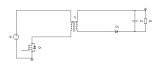
The winding polarity and diode orientation make the secondary rectifier block during primary excitation. A dot alone is insufficient: in this drawing, the primary dotted end is at the positive input and the secondary dotted end is at its local return.
- Switch on: the input is applied across the primary, and primary current ramps up, storing magnetic-field energy, predominantly in the gap of a typical gapped design. The secondary voltage is reversed, so the output diode is blocked. No power reaches the output. The output capacitor alone supplies the load.
- Switch off: the primary current is interrupted. The core’s stored energy must go somewhere, so the voltage across every winding reverses until the output diode conducts, and the energy is dumped into the output capacitor through the secondary.
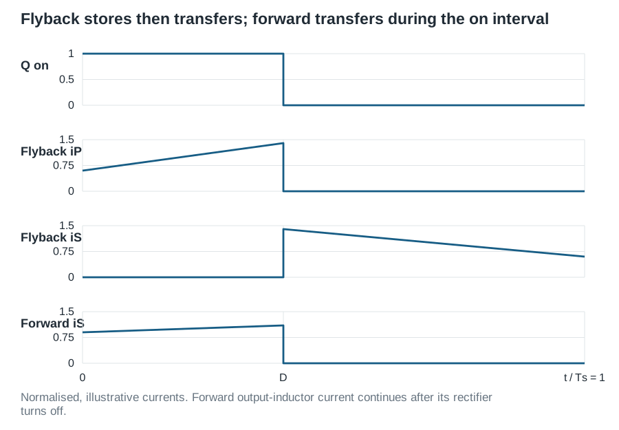
So a flyback transformer is not really a transformer — it is a coupled inductor that stores energy in one interval and releases it in the next. In the ideal interval model, primary and secondary load-current pulses occupy different intervals; real commutation, capacitance and leakage add transition currents. This is why a flyback core needs an air gap: it must store energy, and a gapped core stores far more of it than an ungapped one.
2. The turns ratio and the conversion ratio
Apply volt-second balance to the magnetising inductance, referring everything to the primary. During the on interval the primary sees \(V_g\). During the off interval it sees the output voltage reflected through the turns ratio, \(nV\), where \(n=N_p/N_s\):
\[D V_g=(1-D)\,nV \tag{1}\]which gives the flyback conversion ratio:
\[\boxed{V=\frac{V_g}{n}\cdot\frac{D}{1-D}},\qquad \boxed{D=\frac{nV}{V_g+nV}}. \tag{2}\]This is exactly the buck–boost ratio \(D/(1-D)\) scaled by \(1/n\). The turns ratio gives you a free, lossless gain factor, which is why a flyback handles a 325 V to 5 V conversion comfortably where a buck–boost would need an absurd duty cycle.
The quantity \(nV\) appears constantly in flyback design and has its own name: the reflected voltage or \(V_{\mathrm{OR}}\). For our example with \(n=2\) and \(V=12\ \mathrm{V}\), \(V_{\mathrm{OR}}=24\ \mathrm{V}\).
Switch and diode stress
When the switch is off, its drain sits at the input plus the reflected voltage:
\[V_{\mathrm{DS,off}}=V_g+nV=V_g+V_{\mathrm{OR}} \tag{3}\]and the output diode blocks
\[V_{\mathrm{D,rev}}=V+\frac{V_g}{n}. \tag{4}\]Choosing \(n\) is therefore a direct trade-off: a large \(n\) raises \(V_{\mathrm{OR}}\) and stresses the switch but relaxes the diode; a small \(n\) does the reverse. There is no free choice, and this is the first real design decision in a flyback.
| Input | Duty | \(V_{\mathrm{DS,off}}\) | \(V_{\mathrm{D,rev}}\) |
|---|---|---|---|
| 36 V | 0.400 | 60 V | 30 V |
| 48 V | 0.333 | 72 V | 36 V |
| 72 V | 0.250 | 96 V | 48 V |
At high line the switch already sees 96 V before the leakage spike discussed below. A 150 V MOSFET is the realistic minimum here, and a 100 V Schottky suits the secondary.
3. Sizing the magnetics
| Quantity | Value |
|---|---|
| Input voltage | 48 V nominal; 36–72 V range |
| Output | 12 V, 2.5 A, 30 W (4.8 Ω) |
| Switching frequency | 100 kHz |
| Turns ratio \(n=N_p/N_s\) | 2 |
| Primary magnetising inductance \(L_m\) | 220 µH |
| Output capacitance | 470 µF |
The magnetising current (referred to the primary) is set by the power flow, not by the load directly. Since the input current flows only during the on interval,
\[I_m=\frac{P_{\mathrm{in}}}{V_gD}=\frac{30}{48\times0.3333}=1.875\ \mathrm{A}, \tag{5}\]with the usual ramp during the on time:
\[\Delta i_m=\frac{V_gD}{L_mf_s}=\frac{48\times0.3333}{220\ \mu\mathrm{H}\times100\ \mathrm{kHz}}=0.727\ \mathrm{A}. \tag{6}\]That is a 39 % ripple ratio, a sensible CCM design point. The peak primary current is 2.24 A, and the peak secondary current is \(n\) times larger:
\[I_{\mathrm{sec,pk}}=n\,I_{m,\mathrm{pk}}=4.48\ \mathrm{A}. \tag{7}\]Size the core for \(I_{m,\mathrm{pk}}\) without saturating, and remember that a flyback core stores \(\tfrac12L_mI_{\mathrm{pk}}^2\) of energy every cycle — the air gap is what makes that possible.
The output capacitor works hard
The secondary diode only conducts during the off interval, so the output current is pulsating, exactly as in a boost or buck–boost:
\[\Delta v_o\approx\frac{I_oD}{C f_s}=17.7\ \mathrm{mV}, \qquad I_{C,\mathrm{rms}}\approx I_o\sqrt{\frac{D}{1-D}}=1.77\ \mathrm{A}. \tag{8}\]As always in this family, ripple current rating selects the capacitor, not capacitance. ESR usually dominates the measured ripple.
4. Leakage inductance and the turn-off clamp
Here is the thing that catches every beginner. Equations (1)–(8) assume perfect coupling between primary and secondary. Real windings are not perfectly coupled: a small leakage inductance \(L_{lk}\) stores energy that is not coupled to the secondary and therefore has nowhere to go when the switch turns off.
That trapped energy,
\[E_{lk}=\tfrac12L_{lk}I_{\mathrm{pk}}^2, \tag{9}\]resonates with the switch’s output capacitance and produces a large voltage spike on top of the already-high \(V_g+V_{\mathrm{OR}}\). Left unmanaged it destroys the switch. Every real flyback therefore has a clamp:
- RCD clamp. A diode steers the leakage current into a capacitor, and a resistor bleeds it away as heat. Cheap, universal, and lossy. Size the resistor from the power it must dissipate, \(P\approx E_{lk}f_s\), and set the clamp level comfortably above \(V_{\mathrm{OR}}\) — typically 1.5 to 2 times — so the clamp does not steal real output energy every cycle.
- Active clamp. A MOSFET and capacitor recycle the leakage energy instead of burning it, and can additionally deliver zero-voltage switching. More expensive, considerably more efficient, and now common in compact fast chargers.
For our example, with roughly 2 µH of leakage and a 2.24 A peak, equation (9) gives about 5.5 µJ per cycle — around 0.55 W at 100 kHz, a meaningful fraction of a 30 W converter’s loss budget. The supplied netlist includes an RCD clamp sized on exactly this basis.
Minimising leakage is a winding problem, not a circuit problem: interleave the primary and secondary, keep the windings tightly coupled, and avoid tall, narrow window geometries.
5. CCM or DCM? A genuine design choice
Unlike the non-isolated converters, where DCM is usually something to avoid at light load, flybacks are deliberately designed in either mode.
Discontinuous conduction (DCM) — the core fully empties every cycle:
- The secondary diode turns off at zero current, so there is no reverse-recovery loss.
- The control-to-output response is essentially first order with no right-half-plane zero, which makes the loop far easier to compensate and allows higher bandwidth.
- Peak currents are higher for the same power, raising conduction loss and RMS stress.
Continuous conduction (CCM) — current never reaches zero:
- Lower peak and RMS currents, so better conduction loss and smaller ripple.
- But it inherits the buck–boost’s right-half-plane zero, and diode reverse recovery becomes real.
For this design the boundary sits at
\[P_{\mathrm{boundary}}=V_gD\frac{\Delta i_m}{2}=5.82\ \mathrm{W} \qquad(I_o=0.485\ \mathrm{A}), \tag{10}\]so the converter is in CCM above about 19 % of full load and slides into DCM below it. A controller must remain stable in both, because the plant genuinely changes order at that boundary. This is the single most under-appreciated fact in flyback control.
6. Modelling and closing the loop
In CCM, the flyback is a buck–boost seen through the turns ratio. Working in secondary-referred quantities with \(L_e=L_m/n^2=55\ \mu\mathrm{H}\), the duty-to-output response takes the familiar form
\[G_{vd}(s)=G_{d0}\, \frac{1-s/\omega_{z,\mathrm{RHP}}}{1+\dfrac{s}{Q\omega_0}+\dfrac{s^2}{\omega_0^2}} \tag{11}\]with
\[G_{d0}=\frac{V}{DD'},\quad \omega_0=\frac{D'}{\sqrt{L_eC}},\quad Q=D'R\sqrt{\frac{C}{L_e}},\quad \omega_{z,\mathrm{RHP}}=\frac{D'^2R}{DL_e}. \tag{12}\]Evaluated across the input range:
| Input | Duty | \(f_0\) | \(Q\) | \(f_{z,\mathrm{RHP}}\) | Peak |
|---|---|---|---|---|---|
| 36 V | 0.400 | 594 Hz | 8.42 | 12.5 kHz | 52.5 dB |
| 48 V | 0.333 | 660 Hz | 9.35 | 18.5 kHz | 54.1 dB |
| 72 V | 0.250 | 742 Hz | 10.52 | 31.3 kHz | 56.6 dB |
Two things stand out. The resonant peak is enormous — over 50 dB — because the load resistance is low and damping is light. And the right-half-plane zero is comparatively benign here, worst case 12.5 kHz at low line, so the binding constraint is more the resonance and the switching frequency than the zero. That is specific to this low-voltage, low-impedance output; a high-voltage flyback output behaves differently, so always evaluate (12) for your own design rather than reciting a rule of thumb.
A deliberately slow PI baseline that gives a single gain crossing is
\[G_c(s)=K_p+\frac{K_i}{s},\qquad K_p=1.5\times10^{-3},\quad K_i=1.5, \tag{13}\]crossing over near 13 Hz with a large phase margin. In practice you would use Type II compensation to place a zero near \(f_0\) and a pole above it, and target a crossover of roughly 1–2 kHz — still below one fifth of the worst-case RHP zero.
Practical realities the model does not contain. Isolation means the feedback signal must cross the barrier, almost always through an optocoupler with a TL431 shunt reference on the secondary side. That network adds its own pole and a gain set by the optocoupler’s current transfer ratio (CTR), which varies part to part, with temperature and with age. Budget for CTR spread — it is a frequent cause of a loop that is stable on the bench and marginal in production. Most modern flyback controllers also use peak current-mode control, which tames the resonance and gives cycle-by-cycle protection.
The MATLAB script builds this plant, reports all margins, and sweeps the operating point.
7. Simulate it
Open flyback_open_loop.cir in LTspice and plot V(out), V(sw), I(Lpri) and I(Lsec).
Four observations worth making yourself:
V(sw)has a flat top near 72 V during the off interval. That plateau is \(V_g+V_{\mathrm{OR}}\) — you can literally read the reflected voltage off the waveform.- A spike sits on top of that plateau, clamped by the RCD network. Delete
Dclampand re-run to see how far it would otherwise go. This is the most instructive five seconds in the whole article. I(Lpri)andI(Lsec)never overlap. Primary ramps up while secondary is zero, then they swap. That non-overlap is the definition of flyback operation.I(Lsec)peaks around 4.5 A — twice the primary peak, because \(n=2\).
Then raise RLOAD to 48 Ω (about 3 W) and watch the primary current reach zero before the period ends: the converter has entered DCM, and the output voltage rises above 12 V because the open-loop duty is now wrong for that mode.
The netlist also demonstrates the dot convention directly. Swap the secondary node order from Lsec 0 sec to Lsec sec 0 and the circuit stops being a flyback — the secondary now conducts during the on interval, which is a forward converter, the subject of the next chapter.
8. Where flybacks are used
Low-power offline supplies (roughly under 75 W). Phone chargers, laptop adapters, appliance and TV standby rails, LED drivers. Below about 75 W the flyback’s minimal part count beats everything else, and it dominates the market.
Auxiliary and bias supplies. Almost every larger converter contains a small flyback generating gate-drive and control rails from the DC link — often with multiple outputs, which a flyback provides almost free by adding windings. Cross-regulation between those windings is loose, so the tightest-tolerance rail gets the feedback.
High-ratio conversion. The turns ratio makes 325 V to 5 V routine, which no non-isolated topology manages gracefully.
Where not to use one. Above roughly 100–150 W the peak currents, the RMS stress, the output capacitor ripple and the leakage-clamp loss all become punishing. That is where the forward converter and the bridge topologies take over — they transfer power while the switch conducts, instead of storing it and dumping it.
Further study
Robert W. Erickson and Dragan Maksimović, Fundamentals of Power Electronics, third edition, Springer, 2020, for converter analysis and transformer-isolated topologies. The derivations and numerical example here are presented independently; this article is not a reproduction of the textbook.