
A switching converter contains a switch that changes the circuit thousands of times per second. Yet feedback designers often describe it with a smooth transfer function. Where does that function come from, and what information disappears along the way?
This article works through an ideal boost converter from the two switching states to its small-signal model. It is the mathematical companion to Boost Converter: From Zero to Everything. You need basic circuit laws, differentiation and elementary algebra; the Laplace-transform steps are explained as we use them.
Scope of this draft: a single-phase, diode boost in CCM, ideal components, a resistive baseline load, small switching ripple and perturbations slow compared with switching. Numerical results describe this analytical model, not measured hardware.
On this page: purpose → notation → switching equations → averaging → equilibrium → linearisation → state space → transfer functions → physical meaning → numerical example → validation.
1. What does “small signal” actually mean?
Suppose the output is settled at 24 V. We then increase duty by a tiny amount and ask: how much does the output change, and how quickly?
That is a local question. We are not asking the same model to explain charging an empty output capacitor, a short circuit, or a jump from zero to full power.
For a smooth nonlinear relationship \(y=f(x)\), Taylor expansion around \(X\) gives
\[f(X+\hat x)=f(X)+f'(X)\hat x+\frac12 f''(X)\hat x^2+\cdots. \tag{1}\]When the perturbation is sufficiently small, the first-order term describes the change:
\[\hat y\approx f'(X)\hat x. \tag{2}\]The derivative is a local slope. A small-signal dynamic model applies the same idea to differential equations. Its coefficients depend on the operating point, but the perturbation equations are linear. This lets us use superposition, transfer functions and frequency-response methods for local control design.
There is no universal amplitude that makes a perturbation “small”. Reduce its size and check whether the predicted response converges towards the nonlinear response.
2. Define the circuit, symbols and assumptions
The input feeds an inductor. Its other terminal connects to a low-side switch and the anode of a diode. The diode cathode feeds an output capacitor and resistor in parallel. Inductor current is positive from the source towards the switching node; output voltage is positive relative to the common ground.
| Symbol | Meaning |
|---|---|
| \(v_g, v_o, i_L, d\) | Averaged input voltage, output voltage, inductor current and duty |
| \(V_g, V, I, D\) | Their constant operating-point values |
| \(\hat v_g,\hat v_o,\hat i_L,\hat d\) | Small deviations from that operating point |
| \(L,C,R\) | Inductance, output capacitance and baseline load resistance |
| \(q=D'=1-D\) | Complementary steady-state duty ratio (off-time fraction) |
| \(f_s,T_s\) | Switching frequency and period |
| \(s\) | Laplace variable, with units of inverse seconds |
For the switching equations only, current and voltage denote the instantaneous quantities within each interval. From the averaging step onwards, they denote cycle-averaged quantities.
We assume ideal switches and diode, no inductor resistance or capacitor ESR, a fixed R and CCM throughout the perturbation. We also assume switching ripple is small enough for the usual first-order averaged approximation. These are deliberate simplifications; we will return to their consequences.
3. Write the two switching states
Use the energy-storage laws
\[v_L=L\frac{di_L}{dt},\qquad i_C=C\frac{dv_o}{dt}. \tag{3}\]State A: switch on
The switching node is at ground and the diode blocks. The input voltage appears across L. The capacitor alone supplies the load current \(v_o/R\):
\[\frac{di_L}{dt}=\frac{v_g}{L},\qquad \frac{dv_o}{dt}=-\frac{v_o}{RC}. \tag{4}\]The negative sign in the capacitor equation means its voltage decreases while it supplies the load.
State B: switch off
Inductor current flows through the diode into the output. The inductor voltage is input minus output; capacitor current is inductor current minus load current:
\[\frac{di_L}{dt}=\frac{v_g-v_o}{L},\qquad \frac{dv_o}{dt}=\frac{i_L}{C}-\frac{v_o}{RC}. \tag{5}\]A frequent error is to write \(i_C=i_L\) during the off interval. The load is still drawing current, so it must be subtracted.
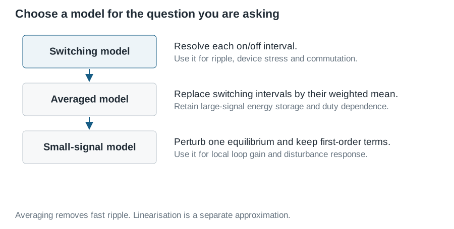
4. Average over a switching period
A switching-period average is defined by
\[\langle x\rangle_{T_s}(t)=\frac{1}{T_s}\int_t^{t+T_s}x(\tau)\,d\tau. \tag{6}\]The averaged state describes the slowly varying envelope of the switching waveform. The small-ripple approximation lets us replace interval state values by this envelope when weighting the two interval equations. We suppress the angle brackets below to keep the notation readable.
The switch is on for a fraction d and off for a fraction \(1-d\). Approximate each averaged derivative by the weighted sum of its two state derivatives:
\[L\frac{di_L}{dt} =d\,v_g+(1-d)(v_g-v_o) =v_g-(1-d)v_o, \tag{7}\] \[C\frac{dv_o}{dt} =d\left(-\frac{v_o}{R}\right) +(1-d)\left(i_L-\frac{v_o}{R}\right) =(1-d)i_L-\frac{v_o}{R}. \tag{8}\]We now have a nonlinear averaged model:
\[\boxed{L\dot i_L=v_g-(1-d)v_o},\qquad \boxed{C\dot v_o=(1-d)i_L-v_o/R}. \tag{9}\]A dot denotes differentiation with respect to time. Fast ripple is no longer resolved. The products \(d v_o\) and \(d i_L\) remain, so averaging has not made the system linear.
The approximation is useful for dynamics well below switching frequency, provided CCM and the small-ripple assumptions remain valid. It is not a general replacement for the switching circuit during startup or mode transitions.
5. Find the operating point
An operating point is a steady solution of the averaged equations. Set both derivatives to zero:
\[0=V_g-qV,\qquad 0=qI-\frac{V}{R}. \tag{10}\]Therefore
\[\boxed{V=\frac{V_g}{q}},\qquad \boxed{I=\frac{V}{Rq}=\frac{V_g}{Rq^2}}. \tag{11}\]The ripple still exists in the switching circuit; “steady” here means that its cycle averages are constant.
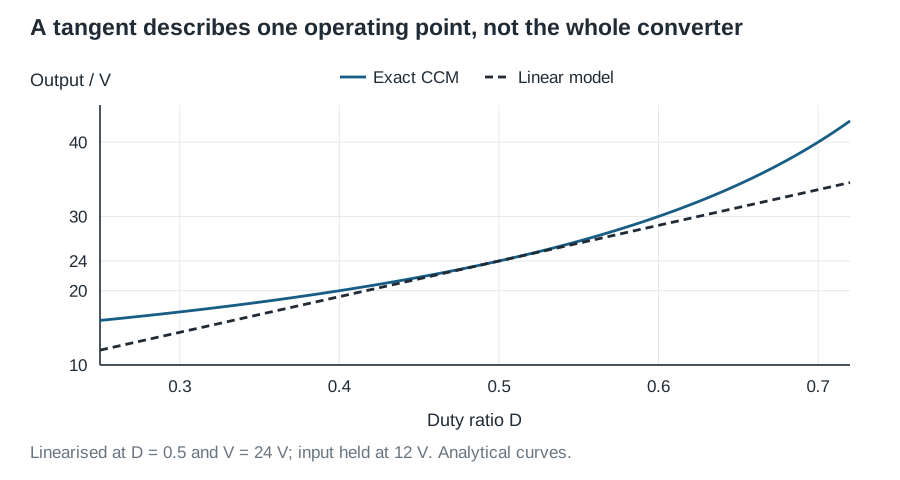
These equilibrium identities are essential. We will use them to remove constant terms during linearisation. Linearising around numbers that do not satisfy equilibrium creates an unwanted forcing term and is not the steady operating-point model intended here.
6. Introduce perturbations and keep first-order terms
Write
\[\begin{aligned} v_g&=V_g+\hat v_g,& v_o&=V+\hat v_o,\\ i_L&=I+\hat i_L,& d&=D+\hat d. \end{aligned} \tag{12}\]A hat means deviation, not derivative. For example, \(\hat d=0.005\) changes duty from 0.500 to 0.505: half a percentage point, or 1% relative to the original duty.
Expand the inductor equation completely
Since \(1-d=q-\hat d\),
\[L\frac{d(I+\hat i_L)}{dt} =V_g+\hat v_g-(q-\hat d)(V+\hat v_o). \tag{13}\]I is constant, so its derivative is zero. Expanding the right-hand side gives
\[L\dot{\hat i}_L =\underbrace{V_g-qV}_{=0} +\hat v_g-q\hat v_o+V\hat d+\hat d\hat v_o. \tag{14}\]The product \(\hat d\hat v_o\) is second order: if both perturbations are scaled by a small factor ε, it scales as ε², while the retained terms scale as ε. Neglect it to obtain
\[\boxed{L\dot{\hat i}_L=\hat v_g-q\hat v_o+V\hat d}. \tag{15}\]Expand the capacitor equation completely
Similarly,
\[C\frac{d(V+\hat v_o)}{dt} =(q-\hat d)(I+\hat i_L)-\frac{V+\hat v_o}{R}, \tag{16}\]so
\[C\dot{\hat v}_o =\underbrace{qI-V/R}_{=0} +q\hat i_L-I\hat d-\frac{\hat v_o}{R}-\hat d\hat i_L. \tag{17}\]Discarding the second-order product gives
\[\boxed{C\dot{\hat v}_o=q\hat i_L-I\hat d-\frac{\hat v_o}{R}}. \tag{18}\]Notice the negative duty term. At the instant duty increases, inductor current has not yet increased, but the fraction of the cycle available to supply the output has decreased.
The complete local model is these two boxed equations. We kept the dynamics, but replaced nonlinear interactions by their first-order behaviour around a specified operating point.
7. Put the equations into state-space form
Choose the energy-storage variables as states:
\[\hat x=\begin{bmatrix}\hat i_L\\\hat v_o\end{bmatrix}. \tag{19}\]Then
\[\dot{\hat x}=A\hat x+B_d\hat d+B_g\hat v_g, \tag{20}\]with
\[A=\begin{bmatrix}0&-q/L\\q/C&-1/(RC)\end{bmatrix},\qquad B_d=\begin{bmatrix}V/L\\-I/C\end{bmatrix},\qquad B_g=\begin{bmatrix}1/L\\0\end{bmatrix}. \tag{21}\]For output voltage,
\[\hat v_o=C_y\hat x,\qquad C_y=\begin{bmatrix}0&1\end{bmatrix}. \tag{22}\]There is no direct feedthrough to output voltage: capacitor voltage cannot jump for finite capacitor current. We use \(C_y\) for the output matrix to avoid confusing it with capacitance C.
The same matrices can be obtained by taking partial derivatives of the nonlinear state equations at equilibrium: \(A=\partial f/\partial x\), \(B_d=\partial f/\partial d\) and \(B_g=\partial f/\partial v_g\). This Jacobian method becomes convenient for more complex converters.
8. Derive the transfer functions by elimination
The Laplace transform turns differentiation into multiplication by s when initial perturbations are zero. This does not set the physical inductor current and capacitor voltage to zero; they start at I and V.
The transformed equations are
\[Ls\hat i_L=\hat v_g-q\hat v_o+V\hat d, \tag{23}\] \[\left(Cs+\frac1R\right)\hat v_o=q\hat i_L-I\hat d. \tag{24}\]Multiply the second equation by Ls and substitute the first:
\[Ls\left(Cs+\frac1R\right)\hat v_o =q\left(\hat v_g-q\hat v_o+V\hat d\right)-LIs\hat d. \tag{25}\]Collect the output terms on the left:
\[\underbrace{\left(LCs^2+\frac LR s+q^2\right)}_{\Delta(s)}\hat v_o =q\hat v_g+(qV-LIs)\hat d. \tag{26}\]Duty-to-output response
Hold input voltage fixed, meaning \(\hat v_g=0\), not \(V_g=0\):
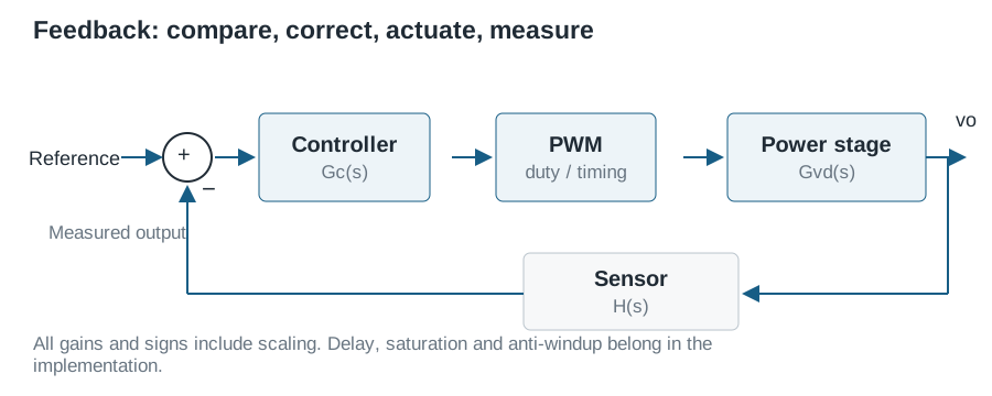
\[\boxed{G_{vd}(s)=\left.\frac{\hat v_o}{\hat d}\right|_{\hat v_g=0} =\frac{qV-LIs}{LCs^2+(L/R)s+q^2}}. \tag{27}\]This plant has units of volts per unit duty. It does not yet include the controller, sensing divider or PWM gain.
Input-to-output response
Instead hold duty fixed:
\[\boxed{G_{vg}(s)=\left.\frac{\hat v_o}{\hat v_g}\right|_{\hat d=0} =\frac{q}{LCs^2+(L/R)s+q^2}}. \tag{28}\]At DC, \(G_{vg}(0)=1/q\), matching the ideal conversion ratio.
Load disturbance and output impedance
Add a small current sink \(\hat i_\ell\) in parallel with the baseline resistor. Positive current means extra current drawn from the output. The capacitor perturbation equation becomes
\[C\dot{\hat v}_o=q\hat i_L-I\hat d-\frac{\hat v_o}{R}-\hat i_\ell. \tag{29}\]Repeating the elimination gives
\[\Delta(s)\hat v_o=q\hat v_g+(qV-LIs)\hat d-Ls\hat i_\ell. \tag{30}\]Thus, defining output impedance with a minus sign so an additional load produces a voltage drop,
\[\boxed{Z_o(s)=-\left.\frac{\hat v_o}{\hat i_\ell}\right|_{\hat d=\hat v_g=0} =\frac{Ls}{\Delta(s)}}. \tag{31}\]The ideal model gives \(Z_o(0)=0\): its fixed-duty CCM DC gain is independent of load. This does not mean the real converter has zero output impedance, or that its transient voltage cannot dip.
For a small resistance change, linearisation of \(v_o/R\) gives an equivalent added current \(\hat i_\ell=-V\hat R/R^2\). A constant-power load has a different incremental characteristic and requires its own load model.
9. Read the physical meaning of the poles and zero
Normalise the duty-to-output expression:
\[G_{vd}(s)=\frac{V}{q} \frac{1-s/\omega_z}{1+s/(Q\omega_0)+(s/\omega_0)^2}, \tag{32}\]where
\[\boxed{\omega_0=\frac{q}{\sqrt{LC}}},\qquad \boxed{Q=Rq\sqrt{\frac CL}},\qquad \boxed{\omega_z=\frac{qV}{LI}=\frac{Rq^2}{L}}. \tag{33}\]The two poles represent coupled inductor and capacitor dynamics. The quality factor describes damping in this ideal resistively loaded model. Inductor resistance and capacitor ESR will change the response.
The numerator is zero at positive \(s=\omega_z\), so this is a right-half-plane (RHP) zero. It is not an unstable pole: the uncompensated ideal plant still has stable poles for positive L, C, R and q.
For a small positive duty step with initially zero perturbations and fixed input,
\[\dot{\hat i}_L(0^+)=\frac VL\hat d>0,\qquad \dot{\hat v}_o(0^+)=-\frac IC\hat d<0. \tag{34}\]Output voltage initially moves down. Eventually it moves up because the steady-state duty-to-voltage gain is positive. This inverse response is why arbitrarily fast boost voltage control is difficult.
At sinusoidal frequency ω,
\[1-\frac{j\omega}{\omega_z} \tag{35}\]has phase \(-\tan^{-1}(\omega/\omega_z)\). Its magnitude rises while its phase lags. A left-half-plane zero would instead add phase lead. Do not cancel the RHP zero with a controller pole at positive s; that introduces an unstable internal mode. For another treatment of the boost model and its RHP zero, see Analog Devices AN-149.
Check the DC gain independently
Differentiate the equilibrium conversion law at fixed input:
\[\frac{\partial V}{\partial D} =\frac{V_g}{(1-D)^2}=\frac Vq=G_{vd}(0). \tag{36}\]This agreement is a useful check on signs and factors of \(1-D\).
10. Substitute the 12 V to 24 V example
Use
\[V_g=12\ \mathrm V,\quad D=0.5,\quad R=19.2\ \Omega, \quad L=150\ \mu\mathrm H,\quad C=330\ \mu\mathrm F. \tag{37}\]The equilibrium is \(V=24\ \mathrm V\) and \(I=2.5\ \mathrm A\). The transfer functions become
\[G_{vd}(s)=\frac{12-0.000375s} {4.95\times10^{-8}s^2+7.8125\times10^{-6}s+0.25}, \tag{38}\] \[G_{vg}(s)=\frac{0.5} {4.95\times10^{-8}s^2+7.8125\times10^{-6}s+0.25}. \tag{39}\]This gives
\[G_{vd}(0)=48\ \mathrm{V/duty},\quad f_0\approx357.7\ \mathrm{Hz},\quad Q\approx14.24, \quad f_z\approx5093\ \mathrm{Hz}. \tag{40}\]For a duty change of 0.005, the predicted eventual voltage change is
\[\hat v_o(\infty)=48\times0.005=0.240\ \mathrm V. \tag{41}\]The exact new ideal CCM equilibrium is
\[\frac{12}{1-0.505}=24.242424\ldots\ \mathrm V. \tag{42}\]The small-signal prediction is close because the perturbation is small. The exact discrepancy is a nonlinear effect, not a simulation error. For a much larger step, from duty 0.5 to 0.6, the linear model predicts a 4.8 V rise whereas the exact equilibrium rises by 6 V.
The initial voltage slope for the 0.005 step is
\[\dot{\hat v}_o(0^+)=-\frac{2.5}{330\times10^{-6}}\times0.005 \approx-37.88\ \mathrm{V/s}. \tag{43}\]That initial negative slope and eventual positive change should both be visible when the averaged model is evaluated at sufficient time resolution.
The downloadable MATLAB script reproduces these transfer functions, plots the duty-step response, and analyses the conservative PI controller used in the main article. It requires Control System Toolbox; native MATLAB execution is pending.
11. Validate the model rather than trusting the algebra alone
Use three complementary checks.
Equilibrium and units. Substitute the operating point into the averaged derivatives: both must be zero. Check the DC gain against the derivative of the static conversion law. Remember that duty is dimensionless and angular frequency is in rad/s.
Small transient comparison. Start the nonlinear averaged model at I and V, apply a small duty step, and compare its change in output with the linear model. Reduce the perturbation by half and compare responses normalised by perturbation amplitude. They should converge as the discarded nonlinear terms become smaller. The full state excursion, including resonance, must stay within the local regime.
Frequency-response comparison. Inject a small sinusoidal duty perturbation into a settled switching model. At each frequency, discard startup transients and measure the fundamental output response relative to injected duty. Compare amplitude ratio and phase with \(G_{vd}(j\omega)\). Repeat at smaller injection amplitude and tighter solver settings. Average or extract the fundamental so switching ripple is not mistaken for the response.
Agreement should be assessed well below switching frequency and within CCM. Near switching frequency, sampling and switching details become significant; an ideal low-frequency model should not be expected to reproduce them.
12. What changes when the converter becomes real?
The derivation provides a starting point, not a universal plant model.
- Inductor resistance: changes equilibrium and damping. For example, add \(-r_Li_L\) to the averaged inductor voltage equation, then solve and linearise again.
- Capacitor ESR: makes terminal output voltage differ from the ideal capacitor state and introduces additional frequency dependence. Define the measured output carefully before deriving the transfer function.
- Nonideal devices: voltage drops, switching losses and nonlinear capacitances alter the operating point and waveforms. Use consistent equations or device models.
- DCM and pulse skipping: require mode-appropriate models; the two CCM intervals are insufficient.
- Current-mode control: adds an inner loop and potentially important sampled dynamics. The outer voltage loop sees a different controlled plant.
- Digital control: adds sensing filters, sampling, computation delay, zero-order hold and PWM-update timing. Discretise the plant/controller and include the actual timing.
- Large events and limits: startup, duty clipping, saturation and protection require nonlinear or switching analysis.
The method remains reusable: define states and operating assumptions, write the circuit equations, average where justified, solve the equilibrium, perturb, linearise and validate. A transfer function is meaningful only together with those assumptions.
Return to the engineering workflow: Boost Converter: From Zero to Everything, including control implementation, simulation, PCB design and prototype measurements.
Further study
Robert W. Erickson and Dragan Maksimović, Fundamentals of Power Electronics, third edition, Springer, 2020. Relevant chapters cover steady-state converter analysis, AC equivalent circuit modelling, converter transfer functions and controller design. The derivations and numerical example on this page are presented independently; this article is not a reproduction of the textbook.