
A lithium battery starts at 12.6 V, sags to 9 V when it is nearly flat, and your electronics need a steady 12 V. A buck cannot help once the input falls below the output. A boost cannot help while the input is still above it. You need a converter that can do both — and that is the buck–boost.
This tutorial follows one 12 V to −12 V, 30 W inverting buck–boost through the same route used for the buck and boost articles: energy flow, component sizing, modelling, feedback, simulation and hardware. It also covers the four-switch non-inverting version, which is what most modern battery products actually use.
First draft — design example, not a validated reference board. The numerical values below are analytical starting points. The accompanying MATLAB script and LTspice netlist are teaching resources; native simulator execution, completed PLECS/Simulink projects, a KiCad board and hardware measurements are not yet included. No efficiency or transient specification is claimed as a measured result.
Reading route: principles → design → stress → models → feedback → non-inverting → simulation → applications.
1. What is a buck–boost converter?
A buck–boost converter produces an output voltage that can be lower or higher than the input. The classical single-switch version uses the same four parts as a buck or a boost — switch, diode, inductor, capacitor — rearranged so that the inductor is never connected to the input and the output at the same time. Its output is inverted: negative with respect to the input ground.
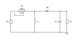
Here Q is a high-side MOSFET. The inductor sits from the switching node to ground. The diode anode faces the output node and its cathode faces the switching node, so current is pulled out of the output node — which is why the output goes negative.
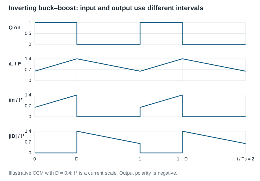
The operating principle is best described as charge then dump. During the on interval the inductor is connected across the input and stores energy, with the output completely disconnected. During the off interval the input is disconnected and the inductor dumps its stored energy into the output capacitor. The inductor is the only thing that links input to output — there is no direct path between them at any instant.
That single fact explains almost everything else about this converter: the output polarity inverts, the conversion ratio is unbounded in both directions, and both the input current and the output current are pulsating.
Analysis conventions
Unless stated otherwise the first calculations assume ideal components, continuous conduction, a resistive load and small switching ripple. To keep the algebra readable, \(V\) denotes the output voltage magnitude; the physical output is \(-V\). Lowercase quantities are time-varying, uppercase are steady-state, and a hat denotes a small perturbation.
Watch one switching cycle
Let \(T_s=1/f_s\) and let duty ratio \(d\) be the fraction of the period for which Q conducts.
Q on, diode off: the input is applied directly across the inductor and its current rises. The output is isolated, so the capacitor alone supplies the load:
\[L\frac{di_L}{dt}=v_g,\qquad C\frac{dv_o}{dt}=-\frac{v_o}{R}. \tag{1}\]Q off, diode on: the input is disconnected. The inductor current continues to flow and is forced through the diode into the output capacitor:
\[L\frac{di_L}{dt}=-v_o,\qquad C\frac{dv_o}{dt}=i_L-\frac{v_o}{R}. \tag{2}\]Note the contrast with a buck, where the inductor feeds the output in both intervals, and with a boost, where the input feeds the inductor in both. Here each source is connected for exactly one interval and never together.
Derive the conversion ratio
Applying inductor volt-second balance over one period,
\[D V_g+(1-D)(-V)=0, \tag{3}\]which rearranges to the defining relation
\[\boxed{V=\frac{D}{1-D}V_g},\qquad \boxed{D=\frac{V}{V+V_g}}. \tag{4}\]Capacitor charge balance gives the inductor current, and this is where the buck–boost starts to hurt:
\[(1-D)I_L=\frac{V}{R}=I_o \qquad\Longrightarrow\qquad \boxed{I_L=\frac{I_o}{1-D}=I_{\mathrm{in}}+I_o}. \tag{5}\]The inductor carries the sum of the input and output currents, not just one of them. At \(D=0.5\) it carries twice the load current.
The ratio \(D/(1-D)\) passes through unity at \(D=0.5\): below that the converter steps down, above it steps up. There is no discontinuity at the crossover, which is exactly the property a battery-powered product needs. As with the boost, driving duty towards one does not give unlimited real output voltage — parasitic resistance takes over long before that.
CCM and DCM
In continuous conduction mode the inductor current never reaches zero. At light load it will, and the converter enters discontinuous conduction, where the gain becomes load-dependent and the model below no longer applies. Because \(I_L\) is large relative to the load current, a buck–boost actually stays in CCM down to a fairly light load — but check it rather than assume it.
2. Turn a requirement into component values
| Quantity | Starting value or objective |
|---|---|
| Input voltage | 12 V nominal; 8–16 V design range |
| Output voltage | −12 V (magnitude 12 V) |
| Maximum output power | 30 W |
| Rated output current | 2.5 A |
| Nominal resistive load | 4.8 Ω |
| Switching frequency | 100 kHz |
| Inductor | 150 µH starting value |
| Output capacitance | 330 µF effective starting value |
| Steady switching-ripple objective | Below 120 mV peak-to-peak; to be verified |
| Topology | Single-switch inverting buck–boost |
An 8–16 V input around a 12 V output is deliberately chosen so the converter must step up and step down within one specification — duty runs from 0.429 at 16 V input to 0.600 at 8 V input, straddling the 0.5 crossover.
Size the inductor
During the on interval the inductor sees the full input voltage:
\[\Delta i_{L,\mathrm{pp}}=\frac{V_gD}{Lf_s}. \tag{6}\]At the nominal point with 150 µH,
\[\Delta i_{L,\mathrm{pp}}=\frac{12\times0.5}{150\times10^{-6}\times100\times10^3}=0.40\ \mathrm{A}. \tag{7}\]From equation (5) the average inductor current is
\[I_L=\frac{I_o}{1-D}=\frac{2.5}{0.5}=5.0\ \mathrm{A}, \qquad I_{L,\mathrm{pk}}\approx5.20\ \mathrm{A}. \tag{8}\]Five amps of inductor current to deliver 2.5 A at 30 W. This is the central cost of the topology and the reason a buck–boost is less efficient than a buck or a boost doing the same job. Check the whole input range: at 8 V input duty rises to 0.6, so \(I_L=2.5/0.4=6.25\ \mathrm{A}\) average with a 6.41 A peak. Size the inductor and the current limit for the low-line condition.
The ideal CCM boundary is at \(I_L=\Delta i_{L,\mathrm{pp}}/2\), giving
\[I_{o,\mathrm{boundary}}\approx(1-D)\frac{\Delta i_{L,\mathrm{pp}}}{2}=0.10\ \mathrm{A}, \tag{9}\]about 1.2 W — so the CCM model holds over most of the useful load range.
Size the capacitor
The output capacitor is on its own for the whole on interval, exactly as in a boost:
\[\Delta v_{o,\mathrm{pp}}\approx\frac{I_oD}{Cf_s}. \tag{10}\]For 330 µF this is about 37.9 mV of capacitive ripple. ESR and diode commutation add to what you actually measure. The RMS current the capacitor must carry is
\[I_{C,\mathrm{rms}}\approx I_o\sqrt{\frac{D}{1-D}}=2.50\ \mathrm{A}, \tag{11}\]which rises steeply at low line. Capacitor ripple-current rating, not capacitance, is usually what selects the part here.
The input side is pulsating too — the switch chops the input current — so a buck–boost needs both a substantial input capacitor and a substantial output capacitor. It is the only member of the basic trio with that penalty.
3. Device stress: the price of flexibility
When Q is off, the switching node sits at the output voltage while its other terminal is at the input. Both the switch and the diode must block
\[V_{\mathrm{DS,off}}=V_{\mathrm{D,rev}}=V_g+V. \tag{12}\]At nominal that is 24 V for a 12 V input and 12 V output, and 28 V at high line — before switching overshoot. Compare this with a buck (stress \(V_g\)) or a boost (stress \(V\)). The buck–boost stacks them.
Combined with the 5 A inductor current, useful first loss estimates are
\[P_{Q,\mathrm{cond}}\approx D\left(I_L^2+\frac{\Delta i_L^2}{12}\right)R_{\mathrm{DS(on)}}, \qquad P_D\approx(1-D)V_FI_L=V_FI_o, \tag{13}\] \[P_{Q,\mathrm{sw}}\approx\frac12 (V_g+V)I_L(t_r+t_f)f_s. \tag{14}\]Both the voltage and the current terms in the switching-loss estimate are worse than in a buck or boost of the same rating. This is why single-switch buck–boost is generally reserved for low power, and why the non-inverting four-switch version dominates above roughly 50 W.
| Quantity | Buck | Boost | Buck–boost |
|---|---|---|---|
| Ideal gain | \(D\) | \(1/(1-D)\) | \(D/(1-D)\) |
| Inductor average current | \(I_o\) | \(I_o/(1-D)\) | \(I_o/(1-D)\) |
| Switch/diode blocking voltage | \(V_g\) | \(V\) | \(V_g+V\) |
| Input current | pulsating | continuous | pulsating |
| Output current into cap | continuous | pulsating | pulsating |
| Output polarity | same | same | inverted |
4. Model it: the worst right-half-plane zero of the three
The averaged CCM equations, with \(v_o\) again the output magnitude, are
\[L\frac{di_L}{dt}=d\,v_g-(1-d)v_o, \qquad C\frac{dv_o}{dt}=(1-d)i_L-\frac{v_o}{R}. \tag{15}\]Perturbing and linearising in the usual way (the method is worked line by line in Small-Signal Modelling from First Principles) gives a duty-to-output transfer function of the standard second-order-with-a-zero form
\[\boxed{G_{vd}(s)=G_{d0}\, \frac{1-s/\omega_{z,\mathrm{RHP}}} {1+\dfrac{s}{Q\omega_0}+\dfrac{s^2}{\omega_0^2}}} \tag{16}\]with the buck–boost parameters, writing \(D'=1-D\),
\[G_{d0}=\frac{V}{DD'},\qquad \omega_0=\frac{D'}{\sqrt{LC}},\qquad Q=D'R\sqrt{\frac{C}{L}},\qquad \omega_{z,\mathrm{RHP}}=\frac{D'^2R}{DL}. \tag{17}\]For this example: \(G_{d0}=48\ \mathrm{V/duty}\), \(f_0\approx358\ \mathrm{Hz}\), \(Q\approx3.56\) and
\[f_{z,\mathrm{RHP}}\approx2.55\ \mathrm{kHz}. \tag{18}\]Why this is the hardest of the three to control
Put the three worked examples side by side — all 30 W at 100 kHz with a 150 µH inductor:
| Buck | Boost | Buck–boost | |
|---|---|---|---|
| RHP zero | none | ≈5.09 kHz | ≈2.55 kHz |
| Resonant peak | ≈40 dB | ≈57 dB | ≈45 dB |
| Plant DC gain | 24 V/duty | 48 V/duty | 48 V/duty |
These are the three articles’ own examples rather than one converter reconfigured, so the load resistances differ (4.8 Ω here, 19.2 Ω for the boost) and the resonant peaks are not a like-for-like comparison. The right-half-plane zero is, because it is set by the topology and the operating point rather than by the chosen load: at 2.55 kHz the buck–boost’s is roughly half the boost’s.
The buck–boost has an inverse response for the same reason the boost does — increasing duty steals time away from the interval that feeds the output, so the output dips before it climbs — but the zero sits at roughly half the boost’s frequency because the energy has to make a full round trip through the inductor. A right-half-plane zero cannot be cancelled by a controller pole, so it sets a hard ceiling on achievable bandwidth.
Worse, the zero moves with operating point. From (17), \(\omega_{z}\propto D'^2/D\), so it marches down as the input falls:
| Input | Duty | \(f_{z,\mathrm{RHP}}\) | \(f_0\) | \(I_L\) |
|---|---|---|---|---|
| 16 V | 0.429 | 3.88 kHz | 409 Hz | 4.38 A |
| 12 V | 0.500 | 2.55 kHz | 358 Hz | 5.00 A |
| 8 V | 0.600 | 1.36 kHz | 286 Hz | 6.25 A |
Low line is the worst corner in every column at once: the lowest zero frequency, the lowest resonance, and the highest inductor current. Any controller must be stable at the lowest zero frequency across the full range, not just at nominal. The supplied MATLAB script prints this sweep.
5. Close the loop
Use the same voltage-mode structure as the earlier articles: sense the output, compare with a reference, and let a compensator set duty. With software reconstructing the output magnitude in volts (\(H=1\)) and the controller producing duty directly, a deliberately slow PI baseline is
\[G_c(s)=K_p+\frac{K_i}{s},\qquad K_p=3.0\times10^{-3}\ \mathrm{V}^{-1},\quad K_i=3.0\ \mathrm{V}^{-1}\mathrm{s}^{-1}. \tag{19}\]This crosses over near 23 Hz with a single gain crossing and a large phase margin. As with the buck, the constraint is that the lightly damped LC peak reaches about 45 dB, so any proportional gain large enough to approach it creates extra unity-gain crossings. Unlike the buck, you could not simply add Type III shaping and cross above resonance anyway — the RHP zero, as low as 1.36 kHz at low line, forbids it.
A realistic design sequence:
- Evaluate the plant across the input range and load range, tracking how \(f_{z,\mathrm{RHP}}\), \(f_0\) and \(G_{d0}\) move. Design for the worst corner.
- Choose a target crossover below roughly one fifth of the minimum RHP-zero frequency. With 1.36 kHz at low line, that means staying under about 270 Hz — a conservative, honest ceiling.
- Use Type II compensation to add phase around crossover; Type III buys little once the RHP zero dominates.
- Add sensing filters, PWM gain and delay, then inspect every crossing and the closed-loop poles.
- Verify line steps, load steps, startup, duty saturation and recovery in a switching model.
Peak current-mode control is the usual practical answer. An inner current loop removes one pole from the voltage-loop plant and gives cycle-by-cycle limiting of that large inductor current — valuable when \(I_L\) is twice the load current. It does not remove the right-half-plane zero, which is a property of the power stage, not of the control scheme.
The MATLAB analysis script builds the plant, reports all margins, plots the inverse step response and sweeps the RHP zero over the input range. Values have been checked numerically; the script has not yet been run in MATLAB.
Digital implementation
Tustin discretisation of the PI gives the usual incremental form
\[u[k]=u[k-1]+\left(K_p+\frac{K_iT_a}{2}\right)e[k] +\left(-K_p+\frac{K_iT_a}{2}\right)e[k-1], \tag{20}\]with coefficients 0.003015 and −0.002985 at \(T_a=10\ \mu\mathrm{s}\). Add duty limits, anti-windup and a feedforward bias
\[d[k]=\operatorname{clip}\bigl(D_{\mathrm{ff}}[k]+u[k],d_{\min},d_{\max}\bigr), \qquad D_{\mathrm{ff}}\approx\frac{V_{\mathrm{target}}}{V_{\mathrm{target}}+v_g}. \tag{21}\]Remember the output is negative: the sensing chain needs a level shift or an inverting amplifier, and getting that sign wrong turns negative feedback into positive feedback.
6. The non-inverting four-switch buck–boost
The inverting topology has three practical problems: the output is the wrong polarity for most loads, the switch is not ground-referenced, and the stress is high. The four-switch non-inverting buck–boost solves all three and is what you will find inside USB-PD adapters, battery chargers and automotive pre-regulators.
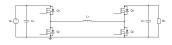
It is literally a synchronous buck cascaded with a synchronous boost sharing one inductor. Q1/Q2 form the buck leg, Q3/Q4 the boost leg. That gives three operating modes:
| Mode | Condition | Behaviour |
|---|---|---|
| Buck | \(V_g\) comfortably above \(V\) | Q3 held on, Q4 off; Q1/Q2 switch with \(V=DV_g\) |
| Boost | \(V_g\) comfortably below \(V\) | Q1 held on, Q2 off; Q3/Q4 switch with \(V=V_g/(1-D)\) |
| Buck–boost | \(V_g\approx V\) | Both legs switch, blended over a transition band |
In a pure buck or boost mode, only one leg needs high-frequency commutation. That can reduce switching loss, but does not guarantee a factor-of-two reduction. The input-leg devices block approximately Vg and the output-leg devices approximately V, before overshoot; all four devices still contribute conduction and drive losses.
The difficulty moves into the control: the transition region near \(V_g\approx V\) must be handled without duty-cycle discontinuities, audible subharmonics or output glitches. Common strategies overlap the two modes across a hysteresis band, or run a genuine four-switch buck–boost mode with a fixed minimum duty on each leg. Mode-transition behaviour, not steady-state efficiency, is what separates a good implementation from a poor one.
Note also that in boost mode the four-switch converter inherits the boost’s right-half-plane zero, while in buck mode it has none. The plant genuinely changes character across the input range — a strong argument for current-mode control with gain scheduling.
7. Simulate it
Download buckboost_open_loop.cir and open it in LTspice. Run the transient analysis and plot V(out), V(sw) and I(L1).
Four things are worth confirming yourself, because they are the ones beginners find surprising:
V(out)settles negative, near −12 V (a little less with the diode drop and winding resistance included).I(L1)averages about 5 A, not 2.5 A — the sum of input and output current.V(sw)swings across roughly 24 V, from near the input rail down to the negative output, confirming the \(V_g+V\) stress.- The settling is slow and ringing, because \(Q\approx3.6\) at 358 Hz. The netlist runs to 30 ms for that reason; shorten it and you will measure a value that has not settled.
Then change DUTY to 0.4 and 0.6 and confirm the output moves to roughly −8 V and −18 V, demonstrating step-down and step-up from one circuit.
For the averaged model in PLECS or Simulink, implement the two derivatives of (15) with two integrators, initialised at 5 A and 12 V. Close the loop with the PI, a duty limiter and explicit anti-windup. To see the right-half-plane zero, apply a small positive duty step to the switching model and watch the output move the wrong way for the first few hundred microseconds before recovering. That single plot teaches the concept better than the algebra does.
Do not use the averaged model to claim switching ripple; averaging has removed it.
8. Where buck–boost converters are actually used
Battery-powered products with an input that crosses the output. A single-cell Li-ion runs 4.2 V down to 3.0 V while the system needs 3.3 V; a 12 V lead-acid runs 14.4 V down to 10.5 V while the load needs 12 V. This is the defining application, and it is why the four-switch topology is so widespread.
USB Power Delivery. A PD source must produce anything from 5 V to 20 V from a fixed intermediate bus, which necessarily crosses the bus voltage. Four-switch buck–boost is the standard answer.
Automotive pre-regulators. A 12 V rail that must survive cold-crank down to 6 V and load-dump above 16 V while holding a stable 12 V for downstream electronics.
LED drivers and small negative rails. The inverting single-switch version remains a cheap way to generate a modest negative supply — bias rails for op-amps, gate-drive rails, or display bias — where the inverted polarity is a feature rather than a problem.
Where not to use one. If the input never crosses the output, do not pay the buck–boost tax. A buck or a boost will do the same job with lower device stress, lower inductor current, one less pulsating port and easier control. The buck–boost earns its place only when the ranges genuinely overlap.
If you need step-up/step-down without polarity inversion and without four switches, the Ćuk, SEPIC and Zeta family offers single-switch alternatives with different ripple and polarity trade-offs. That is the subject of the next article.
Further study
Robert W. Erickson and Dragan Maksimović, Fundamentals of Power Electronics, third edition, Springer, 2020. Relevant chapters cover steady-state converter analysis, AC equivalent circuit modelling and converter transfer functions. The derivations and numerical example here are presented independently; this article is not a reproduction of the textbook.