
The flyback stores energy in the magnetic field of a coupled inductor, usually predominantly in its gap, then transfers that energy to the output during another switching interval. Increasing power raises the demands on stored energy, peak current and temperature; there is no universal power threshold at which the topology stops being usable.
The forward converter transfers power through the transformer while the primary switch conducts. Its output inductor smooths the rectified current, giving a buck-like output stage. The transformer still stores magnetising energy, which must be reset each cycle; that energy is not the main load-energy transfer mechanism.
This article follows the same 48 V to 12 V, 30 W specification at 100 kHz used for the other isolated topologies in this series.
First draft — design example, not a validated reference board. The values are analytical starting points; the LTspice netlist is a teaching resource. Native simulator execution and hardware measurements are not included.
Reading route: principles → the reset problem → design → variants → control → simulation → applications.
1. An isolated buck
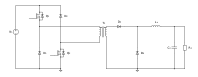
Winding polarity and rectifier orientation are chosen so that positive primary excitation forward-biases the output rectifier. Read the current paths, not the position of a dot alone:
- Switch on: the primary sees \(V_g\), and the secondary immediately produces \(V_g/n\) where \(n=N_p/N_s\). The forward diode
Dfwdconducts and delivers power straight through to the output inductor. Power flows while the switch is on. - Switch off: the secondary voltage collapses,
Dfwdblocks, and the output inductor current freewheels throughDfw, exactly as in a buck.
Look at the node between the two diodes. It sees \(V_g/n\) while the switch is on and approximately zero while it is off — a clean rectangular waveform, precisely what a buck’s switching node produces. Everything downstream is a buck.
Applying volt-second balance to the output inductor:
\[\boxed{V=\frac{V_g}{n}D}. \tag{1}\]Compare this with the buck’s \(V=DV_g\). The transformer contributes a fixed ratio \(1/n\); the duty cycle does the regulating. And because the output inductor conducts continuously into the load, the forward converter inherits the buck’s best property: continuous output current and very low output ripple.
Primary and secondary load-current components flow simultaneously during the forward interval. The transformer therefore does not need to store the full transferred load energy as a flyback coupled inductor does. Core gap, magnetising inductance and winding structure remain design choices; reset and transient flux must still be checked.
2. The reset problem, and where the duty limit comes from
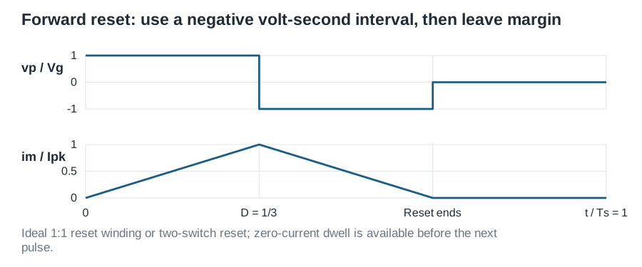
A real transformer still has a magnetising inductance \(L_m\) in parallel with the ideal one. While the switch is on, \(V_g\) is applied across it and the magnetising current ramps up:
\[\frac{di_m}{dt}=\frac{V_g}{L_m}. \tag{2}\]This current does no useful work — it just magnetises the core. And here is the problem: the core must be demagnetised before the next cycle, or the flux staircases upward, cycle after cycle, until the core saturates and the switch fails. Volt-second balance on the magnetising inductance is not optional; it is a survival requirement.
The classical single-switch solution uses a third reset winding with Nr turns and a diode that returns magnetising energy to the input. During reset the primary sees −Vg Np/Nr. If the reset interval occupies a fraction δr of the period, volt-second balance gives the following duty limit. The rest of the off interval can be a zero-magnetising-current dwell.
\[\delta_r=D\frac{N_r}{N_p},\qquad D+\delta_r\leq1 \quad\Longrightarrow\quad D_{\max}=\frac{1}{1+N_r/N_p}. \tag{3}\]With the usual 1:1 reset winding (\(N_r=N_p\)), this gives the famous constraint:
\[\boxed{D\le0.5}. \tag{4}\]The 0.5 limit belongs to the 1:1 reset arrangement and the ideal two-switch reset. Other reset ratios and active-clamp arrangements change the allowable duty. During reset the single-switch device blocks the input plus the reflected reset voltage:
\[V_{\mathrm{DS,off}}=V_g\left(1+\frac{N_p}{N_r}\right)=2V_g \quad\text{for a 1:1 reset winding.} \tag{5}\]At our 72 V maximum input that is 144 V, requiring a 200 V device to switch a 48 V rail. Both of these penalties — the duty ceiling and the doubled voltage stress — are what the variants in section 4 exist to solve.
3. Sizing the example
| Quantity | Value |
|---|---|
| Input voltage | 48 V nominal; 36–72 V range |
| Output | 12 V, 2.5 A, 30 W (4.8 Ω) |
| Switching frequency | 100 kHz |
| Turns ratio \(n=N_p/N_s\) | 4:3 (1.333) |
| Output inductor | 150 µH |
| Output capacitance | 100 µF |
The turns ratio must be chosen so that duty stays under 0.5 at the lowest input:
| Input | Duty | \(V_{\mathrm{DS}}\) (1-switch, 1:1 reset) | \(V_{\mathrm{DS}}\) (two-switch) |
|---|---|---|---|
| 36 V | 0.444 | 72 V | 36 V |
| 48 V | 0.333 | 96 V | 48 V |
| 72 V | 0.222 | 144 V | 72 V |
At 36 V the duty reaches 0.444 — inside the 0.5 limit with a little margin, which is exactly how \(n\) was chosen. Push the input range lower and you would have to reduce \(n\), which raises the secondary voltage and the diode stress.
The secondary square wave is \(V_g/n=36\ \mathrm{V}\). From there the output stage is sized as a plain buck:
\[\Delta i_L=\frac{V(1-D)}{L_of_s} =\frac{12\times0.6667}{150\ \mu\mathrm{H}\times100\ \mathrm{kHz}}=0.533\ \mathrm{A}, \tag{6}\]with \(I_L=I_o=2.5\ \mathrm{A}\) and a 2.77 A peak. The output capacitor sees only the triangular ripple, giving the buck-like \(/8\) result:
\[\Delta v_o\approx\frac{\Delta i_L}{8C f_s}=6.7\ \mathrm{mV}, \qquad I_{C,\mathrm{rms}}\approx\frac{\Delta i_L}{\sqrt{12}}=154\ \mathrm{mA}. \tag{7}\]Compare that with the flyback’s 17.7 mV on 470 µF and 1.77 A of capacitor RMS current. The forward converter achieves lower ripple with less than a quarter of the capacitance and roughly a tenth of the ripple current — because its output current never stops. This, more than anything else, is why the forward topology takes over as power rises.
4. Fixing the weaknesses: two-switch and active clamp
Two-switch forward
Put a switch in both primary legs, driven together, and add two clamp diodes to the opposite rails.
When both switches turn off, the magnetising current flows through the two clamp diodes back into the input. This has three simultaneous benefits:
- Each switch blocks only \(V_g\), not \(2V_g\) — a candidate voltage class must still allow for overshoot, tolerances and the protection limit at 72 V input.
- The magnetising energy is returned to the input rather than dissipated.
- No reset winding is needed, simplifying the transformer.
The duty limit remains \(D\le0.5\), because the reset voltage is still \(V_g\). The cost is a second switch and a high-side gate drive. This is the workhorse configuration for roughly 100 W to 500 W, and it is what the supplied netlist implements.
Active-clamp forward
An active clamp uses an auxiliary switch and capacitor to establish the reset voltage. For the common low-side main-switch arrangement, define the ideal total off-state voltage across the main switch as Vclamp:
\[V_{\mathrm{clamp}}=\frac{V_g}{1-D}, \tag{8}\]which is 72 V at the nominal point. The clamp capacitor voltage itself depends on its connection; it must not be identified with this total switch voltage without drawing that connection. Two useful consequences are:
- Duty can exceed 0.5 in suitable active-clamp arrangements. Switch stress, reset time, flux excursion and controller limits still bound the usable duty.
- Zero-voltage switching becomes available, because the magnetising and leakage energy is used to discharge the switch capacitance before turn-on. Switching loss drops sharply, enabling higher frequencies and smaller magnetics.
The trade-off is complexity: complementary gate drive with carefully chosen dead time, and a clamp voltage that rises with duty, so the device rating must cover the worst case.
| Variant | Switch stress | Duty limit | Reset energy | Typical use |
|---|---|---|---|---|
| Single-switch, reset winding | \(2V_g\) | 0.5 | returned to input | low cost, < 150 W |
| Two-switch | \(V_g\) | 0.5 | returned to input | 100–500 W workhorse |
| Active clamp | \(V_g/(1-D)\) | topology/controller limits | recycled, enables ZVS | high efficiency, high density |
5. Control: the easiest plant in this series
Because the output stage is a buck, the small-signal model is a buck’s — with the input scaled by the turns ratio:
\[\boxed{G_{vd}(s)=\frac{V_g/n}{L_oCs^2+(L_o/R)s+1}}. \tag{9}\]For this example \(G_{d0}=V_g/n=36\ \mathrm{V}\) per unit duty, and
\[f_0=\frac{1}{2\pi\sqrt{L_oC}}=1299.5\ \mathrm{Hz}, \qquad Q=R\sqrt{\frac{C}{L_o}}=3.92. \tag{10}\]Those are exactly the numbers from the buck article — same \(L\), same \(C\), same \(R\), so the same resonance and damping. Only the DC gain differs, scaled from 24 to 36 by the turns ratio. That is not a coincidence; it is the whole point of the topology.
There is no right-half-plane zero. Raising duty raises the output immediately, with no inverse response, because the output inductor feeds the load in both intervals. Of all the isolated converters here, the forward is the easiest to compensate, and a Type III compensator can place the crossover above resonance to reach a genuinely fast loop — typically \(f_s/10\), or about 10 kHz.
The practical caveats are the same as for any isolated converter: the feedback must cross the isolation barrier through an optocoupler and reference, adding a pole and CTR tolerance, and the plant DC gain \(V_g/n\) moves proportionally with input voltage, so evaluate margins at high line where the gain is largest.
6. Simulate it
Open forward_2sw_open_loop.cir and plot V(out), V(n1), I(Lo) and I(Lpri).
V(n1)is a clean rectangle switching between about 36 V and 0. That is the isolated buck’s switching node — compare it directly with the buck article’sV(sw).I(Lo)is a triangle centred on 2.5 A with about 0.53 A of ripple, never touching zero.- Measure the voltage across each switch, rather than treating one node voltage as both switch stresses. Ideal reset clamps the winding terminals to the rails; real parasitics create overshoot.
I(Lpri)contains a small ramp riding on the reflected load current — that ramp is the magnetising current, and it returns to zero each cycle.
In the ideal teaching model, increasing duty beyond the reset allowance should reveal a persistent volt-second error and increasing magnetising-current offset. The supplied linear coupled inductors do not model saturation, so they cannot demonstrate a real core entering saturation or predict switch failure. Add a validated nonlinear magnetic model before making that claim.
7. Where forward converters are used
Mid-power isolated supplies, roughly 75 W to 500 W. Industrial and instrumentation power supplies, telecom rails, server and embedded-system supplies — the band where a flyback’s stored-energy penalty bites but a full bridge is overkill.
Telecom 48 V distributed power. The two-switch forward is a classic choice for converting a −48 V telecom bus to intermediate rails, exactly the specification worked here.
Applications needing low output ripple. Because the output current is continuous, the forward converter produces far cleaner rails than a flyback for the same capacitance — valuable for analogue, RF and sensor supplies.
Selection boundary. Compare a forward design with flyback and double-ended alternatives using the actual voltage range, current stress, reset allowance, magnetics and loss budget. Single-ended excitation uses a different flux excursion from bipolar excitation; it does not establish a universal power cutoff. The next chapter develops push–pull, half-bridge and full-bridge alternatives.
Further study
Robert W. Erickson and Dragan Maksimović, Fundamentals of Power Electronics, third edition, Springer, 2020, for transformer-isolated converter analysis and core reset. The derivations and numerical example here are presented independently; this article is not a reproduction of the textbook.