
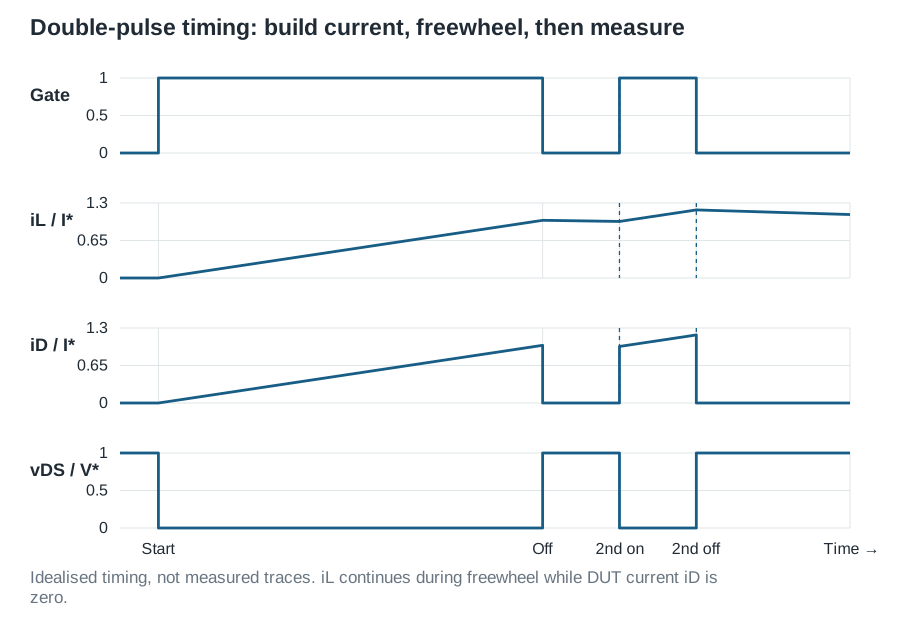
The double-pulse test (DPT) creates a switching event at a chosen voltage, current and initial temperature without continuously operating a complete converter. The first pulse establishes inductor current. The interruption establishes a commutating-device condition. The second pulse reveals turn-on behaviour under that condition.
It is a controlled experiment on a device and its commutation circuit. The result depends on the opposing device, gate driver, layout and measurement system. This tutorial follows the static electrical baseline in the characterisation series.
1. Draw the current paths before choosing instruments
Use a low-side n-channel MOSFET DUT. Connect its source to the negative DC rail and its drain to switching node SW. Connect the load inductor from the positive rail to SW. Connect the freewheel diode with anode at SW and cathode at the positive rail. An upper MOSFET body diode can provide this path when its gate is held off.
| Interval | Conducting path | Physical result |
|---|---|---|
| First pulse | Positive rail → inductor → DUT → negative rail | Inductor current rises |
| Off interval | Positive rail → inductor → SW → freewheel diode → positive rail | Current circulates and decays slowly |
| Second turn-on | Current commutates from freewheel path into DUT | Turn-on overlap, capacitive commutation and possible diode recovery |
| Second turn-off | Current transfers back into freewheel path | Turn-off overlap and voltage overshoot |
Place the pulse-energy DC capacitor close to the semiconductor pair. During fast commutation, the capacitor, DUT and opposing device form the critical loop; the remote bench supply does not behave as an ideal source at the device terminals. For a GaN upper switch, off-state reverse channel conduction can provide the freewheel path, subject to its device-specific gate conditions. Tektronix’s DPT introduction illustrates the basic sequence.

2. Derive the pulse durations
During the first pulse, neglect resistance, DUT voltage drop and bus droop initially:
\[L\frac{di_L}{dt}\approx V_{DC},\qquad t_1\approx\frac{L(I_{\mathrm{target}}-I_0)}{V_{DC}}. \tag{1}\]For a teaching calculation, 48 V, 100 µH, zero initial current and a 10 A target give \(t_1=20.83\ \mu\mathrm{s}\). Check the inductor’s incremental inductance and saturation current at the actual operating point.
With freewheel drop \(V_F\) and loop resistance \(R_f\),
\[L\frac{di_L}{dt}=-(V_F+R_fi_L). \tag{2}\]For a short off interval, the approximate reduction is \(\Delta I\approx(V_F+R_fI)t_{\mathrm{gap}}/L\). A 1 V drop over 2 µs in 100 µH gives 0.02 A when resistance is neglected. Measure the actual second-pulse current; it is the relevant turn-on test condition.
The second pulse must be long enough for the chosen extraction windows and short enough to respect current and thermal limits. Its current rises again, so second turn-on and second turn-off do not automatically occur at equal current. After the last pulse, provide a controlled path for remaining inductor energy and verify recovery before repetition.
3. Bound the available energy
The stored energies are
\[E_L=\frac12LI^2,\qquad E_C=\frac12C_{DC}V_{DC}^2. \tag{3}\]The teaching inductor holds 5 mJ at 10 A. The local bus capacitor can contain much more. Use a rated enclosed fixture with discharge verification, appropriate interlocks and fault containment; a current-limited supply cannot interrupt energy already stored locally.
Before raising voltage, verify gate polarity, off bias, pulse count and driver behaviour at low energy. Establish an initial junction temperature by equilibration and a documented temperature measurement; check whether the first pulse heats the DUT enough to alter the second-pulse result.
4. Make voltage and current refer to the same event
Measure \(v_{DS}\) at the specified package terminals, \(v_{GS}\) relative to the Kelvin-source reference where provided, and DUT current with a suitable shunt or probe. A source shunt may contain gate-return or displacement current depending on its placement; document what crosses the measurement boundary.
Select differential/common-mode ratings, bandwidth, noise and capacitance together. High DC common-mode rejection does not establish adequate rejection during a fast switching edge. Minimise sensing-loop area. A probe changes the circuit through its input capacitance, and a current fixture adds inductance. These effects are discussed in TI’s high-speed measurement note.
Correct voltage/current offsets and relative propagation delay using a documented deskew procedure. Do not slide traces until switching energy appears plausible: physical waveforms need not have coincident edges. Tektronix’s deskew explanation describes why relative channel delay changes energy extraction.
5. Define switching energy before integrating
With positive current entering the DUT drain, the measured drain-port power and energy are
\[p_D(t)=v_{DS}(t)i_D(t),\qquad E_D[a,b]=\int_a^b p_D(t)\,dt. \tag{4}\]Define turn-on and turn-off explicitly:
\[E_{\mathrm{on}}=\int_{t_{\mathrm{on},a}}^{t_{\mathrm{on},b}}v_{DS}i_D\,dt, \qquad E_{\mathrm{off}}=\int_{t_{\mathrm{off},a}}^{t_{\mathrm{off},b}}v_{DS}i_D\,dt. \tag{5}\]Publish the rule locating every endpoint, the included ringing/tail interval, filtering and any conduction-baseline subtraction. Standardised extraction rules depend on device category and document edition; software defaults alone are insufficient evidence of compliance. Keysight’s extraction documentation shows why the selected convention matters.
For sampled traces, use the trapezoidal sum
\[E_D\approx\sum_{k=a}^{b-1} \frac{p_k+p_{k+1}}{2}(t_{k+1}-t_k). \tag{6}\]Retain negative power portions; clipping them changes the energy balance. The port integral includes changes in internally stored electrical energy and is not automatically equal to heat generated during a single transition. Gate-port energy and the opposing device’s energy also require consistent accounting. When using measured switching energies in a converter loss model, identify whether capacitance charging and recovery-related overlap are already included before adding separate \(E_{\mathrm{oss}}\) or recovery terms.
6. Separate recovery charge from total commutation current
Let positive diode current flow anode-to-cathode. An experimentally defined reverse-charge integral is
\[Q_{\mathrm{rev}}=-\int_{t_z}^{t_r}[i_D^{\mathrm{diode}}(t)-i_{\mathrm{baseline}}(t)]\,dt. \tag{7}\]Here \(t_z\) is the defined zero crossing and \(t_r\) the documented recovery endpoint. State the baseline and whether capacitive displacement current remains included. DUT turn-on current also contains load current; its entire spike cannot be labelled diode recovery without identifying the constituent paths.
Silicon and SiC MOSFET body diodes can exhibit minority-carrier recovery. SiC Schottky diodes have principally capacitive reverse transients. Enhancement-mode GaN HEMTs do not have the silicon MOSFET’s minority-carrier body diode, but their capacitances and reverse-conduction interval still affect commutation. Cascode packages require consideration of their internal silicon device. Avoid treating every reverse transient as identical \(Q_{rr}\) physics.
7. Turn the test into a design dataset
For an initial overshoot estimate,
\[\Delta V\approx L_{\mathrm{loop}}\left|\frac{di}{dt}\right|. \tag{8}\]At 10 nH and 1 A/ns this gives 10 V. Ringing and distributed parasitics can invalidate a single-inductance extraction; use this relation as a diagnostic estimate.
| Sweep | Keep documented | Extract |
|---|---|---|
| Bus voltage and load current | Actual values at each edge | Energy surfaces, peak stresses |
| Initial temperature | Equilibration and pulse heating | Temperature dependence |
| Gate resistance/bias | Driver and opposing-device settings | Slew rate, overshoot, losses |
| Off interval | Freewheel path and current history | Recovery and reverse-conduction effects |
Repeat selected points across samples. Reprocess with plausible deskew uncertainty and modest window changes to expose fragile energy estimates. Preserve raw traces, fixture photographs, calibration settings and extraction code. These records make the result reproducible and support the next study of charge, capacitance and dynamic on-resistance.