
A transistor can have a low static on-resistance and still produce substantial switching loss. Charge must move through its gate and output terminals, while the previous blocking condition can affect its subsequent conduction behaviour. Three complementary experiments are therefore needed: capacitance versus bias, gate charge during switching, and on-resistance following a defined stress history.
This chapter extends double-pulse testing within the device-characterisation series. The calculations below illustrate the definitions; they are not measured device data.
1. Interpret capacitance as a local derivative
For a charge-storage element with charge \(q(v)\),
\[C_{\mathrm{diff}}(v)=\frac{dq}{dv},\qquad i(t)=C_{\mathrm{diff}}(v)\frac{dv}{dt}. \tag{1}\]A small sinusoidal excitation around a DC bias measures local incremental behaviour. If the applied AC amplitude is too large, the measurement samples a changing capacitance over the cycle rather than the intended local value.
Under the conventional three-capacitance MOSFET representation,
\[C_{\mathrm{iss}}=C_{gs}+C_{gd},\qquad C_{\mathrm{oss}}=C_{ds}+C_{gd},\qquad C_{\mathrm{rss}}=C_{gd}. \tag{2}\]These quantities are measured with specified terminal connections, bias and frequency. Their simple decomposition is an equivalent-circuit description; terminal-charge models provide a more general treatment when multiple voltages change together. Infineon’s capacitance explanation describes these data-sheet quantities.
Use a capacitance analyser with a suitable bias fixture. Perform the required open/short compensation at the fixture plane, connect terminals according to the extraction method, and sweep DC bias. Record AC amplitude, frequency, temperature, equivalent-series/parallel convention and leakage conductance. Repeat at selected frequencies to identify dispersion or a fixture resonance. Do not extrapolate a high-frequency fixture artefact into a physical capacitance curve.
2. Derive charge and energy by integration
With gate and source connected as required for the output-capacitance measurement, integration of equation (1) gives
\[Q_{\mathrm{oss}}(V)=\int_0^V C_{\mathrm{oss}}(v)\,dv. \tag{3}\]Since incremental stored energy is \(dE=v\,dq\),
\[E_{\mathrm{oss}}(V)=\int_0^V vC_{\mathrm{oss}}(v)\,dv. \tag{4}\]The voltage weighting makes energy and charge different quantities. Only a voltage-independent capacitance gives both \(Q=CV\) and \(E=CV^2/2\) using the same C. Infineon’s output-capacitance FAQ distinguishes energy-related effective capacitance from the point value.
Consider an illustrative piecewise capacitance: 1 nF from 0 to 50 V, then 0.2 nF from 50 to 400 V. Equation (3) gives 120 nC; equation (4) gives 17 µJ. Using only the 400 V capacitance would give 80 nC and 16 µJ. The error differs because the two integrals weight the curve differently.
Useful equivalent values at the chosen endpoint are
\[C_Q(V)=\frac{Q_{\mathrm{oss}}(V)}{V},\qquad C_E(V)=\frac{2E_{\mathrm{oss}}(V)}{V^2}. \tag{5}\]The example gives 300 pF and 212.5 pF. A commutation-time estimate often needs charge; an energy balance needs energy. Stored energy is not universally dissipated at each transition: the circuit may recover part of it, and measured switching-energy conventions may already include relevant contributions.
3. Measure gate charge along a switching trajectory
Gate charge is obtained from measured gate current:
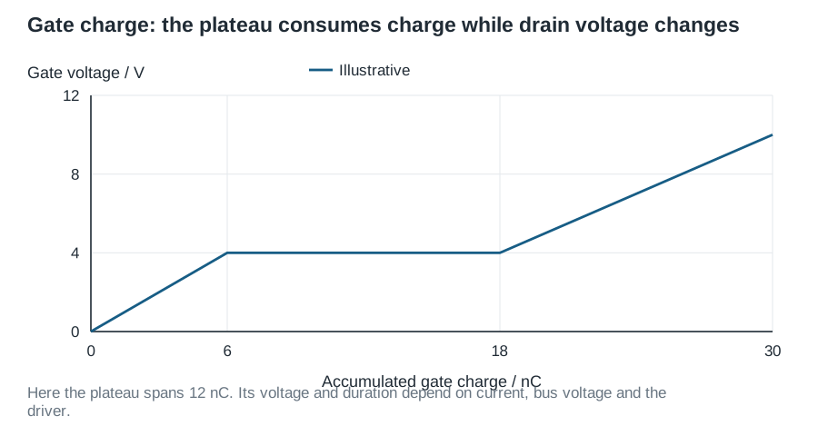
\[Q_g(t)=\int_{t_0}^{t}i_g(\tau)\,d\tau. \tag{6}\]Apply the specified drain voltage and load current, drive the gate through a characterised current source or driver, and measure gate current and gate voltage simultaneously. Remove current offset before integration. Define the gate-voltage endpoints and the time reference. Plot \(v_{GS}\) against accumulated charge together with the drain-voltage trajectory.
During the drain-voltage transition, gate-drain charge transfer often creates a plateau-like region. Its shape depends on device physics, current and external circuit. A single \(C_{\mathrm{iss}}\Delta V_{GS}\) calculation generally cannot reproduce this trajectory because \(v_{DS}\) also changes.
With approximately constant plateau current,
\[t_{\mathrm{Miller}}\approx\frac{Q_{gd}}{I_{g,\mathrm{plateau}}}. \tag{7}\]For an illustrative 12 nC and 0.6 A, the estimate is 20 ns. Driver output impedance, gate resistance and source inductance modify the actual current. Treat the estimate as a starting point and compare it with measured waveforms. Gate-charge extraction is described in Keysight’s parameter documentation.
4. Give dynamic on-resistance a time reference
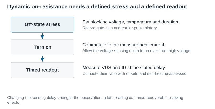
Dynamic on-resistance is the conduction resistance measured after a specified electrical history, at a specified delay after turn-on:
\[R_{\mathrm{on,dyn}}(t_d)=\frac{v_{DS,\mathrm{on}}(t_d)}{i_D(t_d)},\qquad k_{\mathrm{dyn}}(t_d)=\frac{R_{\mathrm{on,dyn}}(t_d)}{R_{\mathrm{on,ref}}}. \tag{8}\]Define the reference using matched current, gate voltage and junction temperature, with documented recovery/preconditioning. Otherwise heating or gate underdrive can be mistaken for a trapping-related increase.
The instrument must resolve a small on-state drop immediately after a large blocking voltage. A protected clamp or specialised measurement channel can preserve low-voltage resolution, but its offset, recovery time and loading become part of the experiment. Keysight’s dynamic-resistance measurement article discusses a clamp-based implementation.
First validate clamp recovery against a known low-voltage signal after a representative high-voltage excursion. Then apply the off-state stress, turn on at controlled current and sample only after both the measurement channel and the defined gate-drive condition have settled. Report that delay: waiting longer can miss fast recovery. If settling obscures the desired interval, identify it as unmeasured rather than extrapolating an apparent peak.
5. Construct a reproducible comparison
| Experiment | Essential sweep | Common false interpretation |
|---|---|---|
| Capacitance | DC bias, frequency, temperature | One point represents the entire voltage swing |
| Gate charge | Drain voltage, current, gate endpoints | Plateau charge is constant across operating conditions |
| Dynamic resistance | Stress voltage/duration, delay, temperature | Clamp recovery or self-heating is intrinsic degradation |
Measure both repeatability and history dependence. Preserve raw voltage/current traces, recovery intervals and calibration records. Enhancement-mode GaN HEMTs have no minority-carrier body-diode recovery, but this does not eliminate output charge, reverse-conduction loss or dynamic-resistance concerns. These are distinct mechanisms and need distinct model parameters.
Use capacitance/charge data to build a charge-consistent switching model. Use dynamic-resistance measurements only over the characterised stress and timing range. Recheck the model against withheld operating points and connect its loss predictions to the thermal-impedance model before drawing temperature or lifetime conclusions.