
A static characteristic describes the relation between terminal voltages and currents after electrical transients have settled. It does not necessarily require a continuous DC experiment. A short, settled measurement pulse can reveal an approximately isothermal characteristic more accurately than a long sweep that heats the die.
This article develops the electrical baseline for the power-semiconductor characterisation series. The baseline is also the reference against which later ageing or switching-induced changes are compared.
1. Define the device and the measurement conditions
Use an enhancement-mode n-channel MOSFET as the first example. Let \(v_{DS}=v_D-v_S\), \(v_{GS}=v_G-v_S\), and let positive \(i_D\) enter the drain. The measured relation is more completely written as
\[i_D=F(v_{DS},v_{GS},T_j,\mathcal H), \tag{1}\]where \(T_j\) is junction temperature and \(\mathcal H\) denotes relevant bias and thermal history. Recording this history is particularly useful when hysteresis or charge trapping is present.
State the package, sample identifier, gate bias, pulse width, sampling delay, repetition interval and temperature method. Data-sheet comparisons must use matching conditions; a typical curve is not a guaranteed production limit. Nexperia’s data-sheet guide explains the distinction between ratings, characteristics and their specified conditions.
2. Measure resistance with separate force and sense paths
A two-wire measurement includes device, leads and contacts:
\[R_{\mathrm{2w}}=R_{\mathrm{device}}+R_{\mathrm{leads}}+R_{\mathrm{contacts}}. \tag{2}\]Use one pair of conductors to force drain current and a separate, high-impedance pair to sense voltage at the intended device terminals. The sense pair carries negligible current, so its lead drop is negligible. Define that reference plane: package-level resistance still includes internal package conductors. A Kelvin-source pin provides a gate reference that avoids shared external power-source impedance; it does not automatically remove every package resistance from a drain-source measurement.
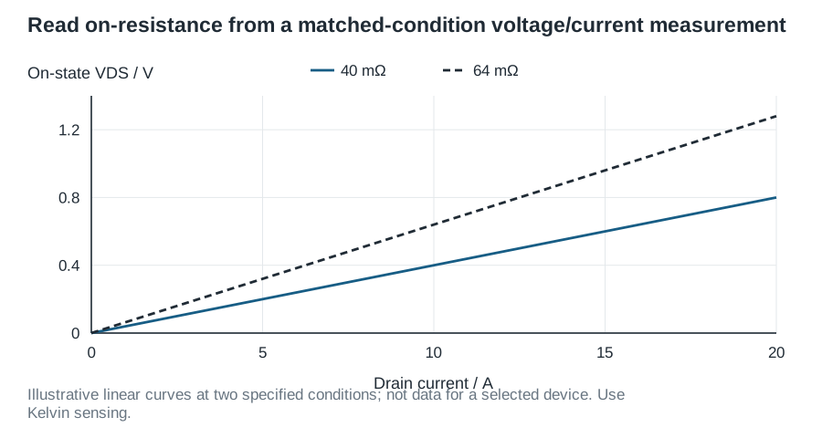
With the channel fully enhanced at the specified gate bias, extract
\[R_{DS(\mathrm{on})}=\frac{V_{DS,\mathrm{sense}}}{I_D}. \tag{3}\]For an illustrative 10 A pulse and 0.120 V sensed drop, the result is 12 mΩ. An additional 3 mΩ of fixture resistance would make a two-wire reading 15 mΩ, a 25% error. These are teaching values, not measurements of a particular component.
Two source-measure channels can provide gate bias and pulsed drain excitation. Verify the actual pulse and settling rather than relying exclusively on programmed settings. Keithley’s on-state measurement discussion describes the need for Kelvin connections and low-voltage measurement capability.
3. Separate electrical settling from self-heating
Choose a sampling window after ringing and source-measure settling, but before appreciable temperature rise. There may be no suitable window if the fixture is slow or the pulse dissipates too much power; improve the setup instead of assuming the requested temperature.
For approximately constant pulse power and the thermal boundary condition represented by the transient impedance,
\[\Delta T_j(t_p)\approx P\,Z_{\mathrm{th}}(t_p). \tag{4}\]Thus 1.2 W and 0.2 K/W give a 0.24 K rise. The assumed impedance must correspond to the package, mounting and time interval; it cannot be selected simply to make heating appear small. Repeat with shorter pulses and longer recovery intervals to test whether extracted resistance changes systematically. Pulsed I–V reduces self-heating, as discussed in Tektronix’s measurement application note.
Control the thermal stage, allow equilibration and document how stage temperature relates to \(T_j\). Use the junction-temperature tutorial when this difference matters.
4. Build output and transfer characteristics
An output family sweeps \(V_{DS}\) at several fixed \(V_{GS}\) values. A transfer characteristic sweeps \(V_{GS}\) at a stated \(V_{DS}\). Respect the pulsed safe operating area throughout: combining individually permitted voltage and current values does not establish an allowed operating point.
The local transconductance and output conductance are
\[g_m=\left.\frac{\partial I_D}{\partial V_{GS}}\right|_{V_{DS},T_j},\qquad g_{ds}=\left.\frac{\partial I_D}{\partial V_{DS}}\right|_{V_{GS},T_j}. \tag{5}\]Estimate derivatives using a documented local fit, retaining the raw curve. Differentiating adjacent noisy samples can produce implausible peaks. Repeat selected points in reverse sweep order to expose heating, settling or history dependence.
Threshold voltage is the gate voltage at a defined small drain-current criterion and drain-bias configuration. It identifies a measurement point near conduction onset. It is not the gate-drive voltage required to achieve the specified low on-resistance. For IGBTs and diodes, measure \(V_{CE(\mathrm{sat})}(I,T)\) or \(V_F(I,T)\) instead of forcing a resistive model across the entire range.
5. Measure leakage and blocking behaviour deliberately
For drain leakage, specify off-state gate bias, drain voltage, temperature and settling time. For gate leakage, specify drain/source connections and gate polarity. Clean insulation surfaces, shield sensitive nodes and distinguish guarding from protective grounding. Measure fixture leakage without the DUT where practical; subtract a baseline only when its stability and relevance have been demonstrated.
Breakdown extraction is a separate, current-limited protocol: ramp the specified voltage toward the defined small-current criterion, stop at the limit and record compliance behaviour. Use the device’s documented method and a rated enclosed fixture. Supply compliance does not eliminate discharge energy from cables or local capacitance. Do not turn a routine leakage sweep into an unplanned avalanche experiment; robustness testing has different objectives.
6. Report uncertainty and produce a usable model
For independent voltage and current uncertainties in equation (3), first-order propagation gives
\[\frac{u_R}{R}\approx \sqrt{\left(\frac{u_V}{V}\right)^2+ \left(\frac{u_I}{I}\right)^2}. \tag{6}\]At 120 mV, a 1 mV voltage uncertainty and 0.5% current uncertainty give approximately 0.97% combined relative uncertainty before temperature, contacts and repeatability are included. Correlated errors require covariance terms.
| Measurement | Controlled variables | Retained evidence |
|---|---|---|
| On-state resistance/drop | Current, gate bias, temperature, pulse timing | Settled waveforms and Kelvin reference plane |
| Output/transfer curves | Bias grid, compliance, sweep order | Raw families and derivative fit settings |
| Threshold | Current criterion, drain connection, history | Extraction rule and repeat readings |
| Leakage/blocking | Bias, temperature, settling, fixture leakage | Compliance events and baseline checks |
Fit a conduction table over the measured current, gate-bias and temperature range. Reserve some measured points for validation. A model that reproduces fitted data but fails these withheld conditions needs revision. Continue with double-pulse testing to determine what changes during switching.